ISSCC Notes
This file would essentially serve as a note-taking platform for the ISSCC 2024 conference.
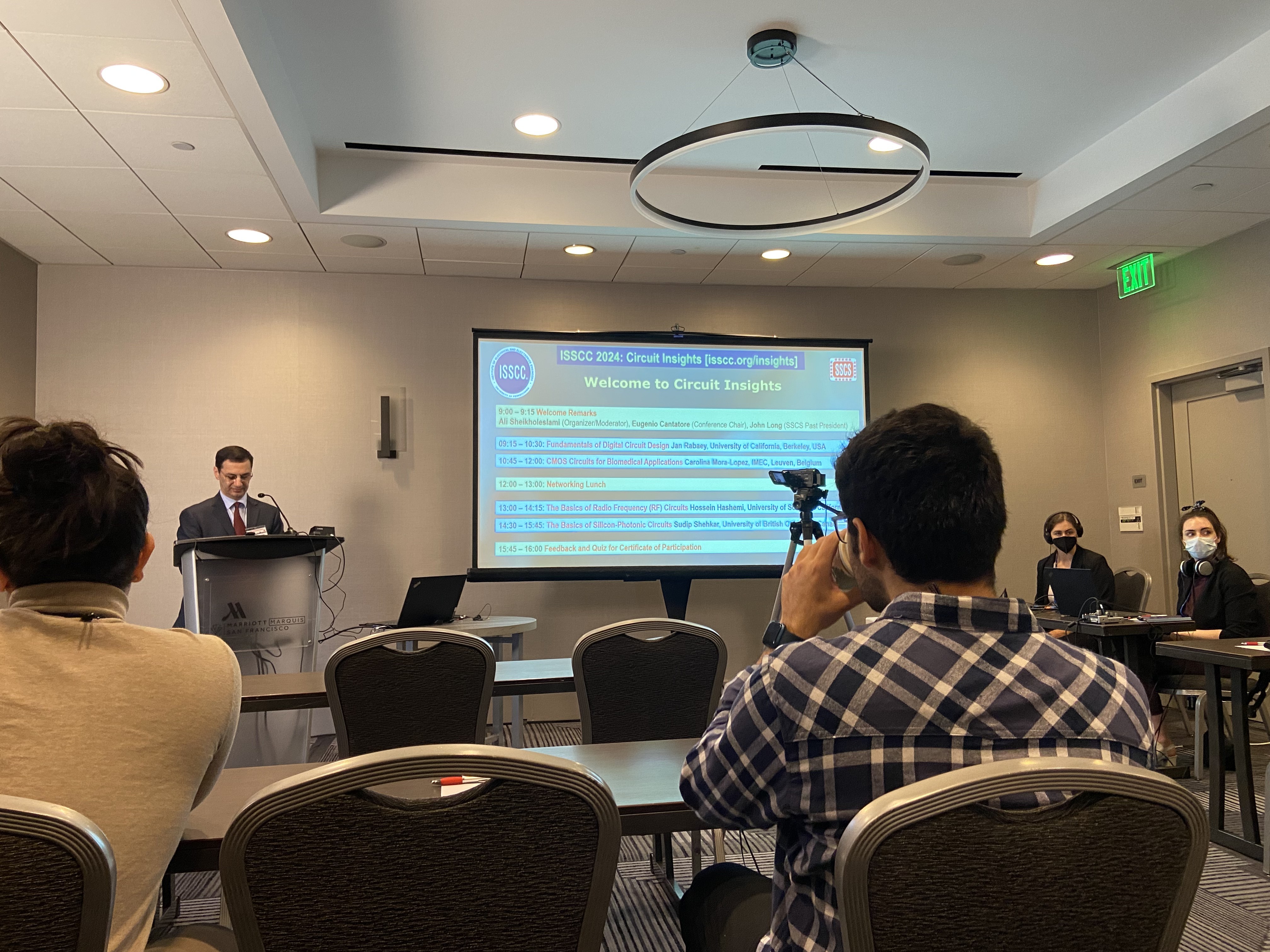
ISSCC Circuit Insight, Feb 17th 2024
The ISSCC Circuit Insight targets fresh grads/graduating undergrads to get a sense of basic circuit theory, industrial trends and future prospects.
There are four key talks for today, which respectively covers digital, analog, RF and photonic circuits.
Fundamentals of Digital Circuit Design
Jan Rabaey
Circuit industry and successes
Boolean Algebra
Circuit Components
Converting voltage signals to 1/0 units.
Defining a threshold.
Example: an inverter
- Nonlinear
- Noise Rejection
- Noise Margins
- Regeneration
- No accumulation of noise in complex circuits
- Contrast with analog circuits
Digital circuits treat transistors as switches. (3-terminal devices)
- when G is high
- $R_{sw} = \infty $ when G is low
CMOS circuits
Non-ideal:
- when on, a few kilo ohms
- Not infinite when off
Speed and Power
Speed of RC networks limit the performance.
Dynamic power and static power due to switching and leakage.
Modularity and Hierarchy
Libraries of common gates/functions
Interfaces are built in such a way.
Delays and power are added linearly.
Composite functions
Timing and Sequential Circuits
Concept: Event -> Asynchronous design. (Clockless)
- Cons: complicated
- Event Driven, relative to changes
Synchronous
- Time reference
Synchronization
- Building blocks: FFs
- Passes signals by 1 register at a time
- Setup time: clock is not too fast
- Hold time
- Timing margins
- Skewed clocks
- Wired RC delays
- Jitters, uncertainties
- Optimize clock distribution network
Memory
- Bistability
- CMOS is inherently compatible
- Store charge, trapped charge
- Latch, DRAM, Flash
Verification
- Functionality
- Signal Noise Margins
- Timing margins
- Optimization and repeatition
Q: how can we mitigate Jitter?
R: Optimize layouts, adding buffers
Q: How worthy is it to implement EDA for async designs?
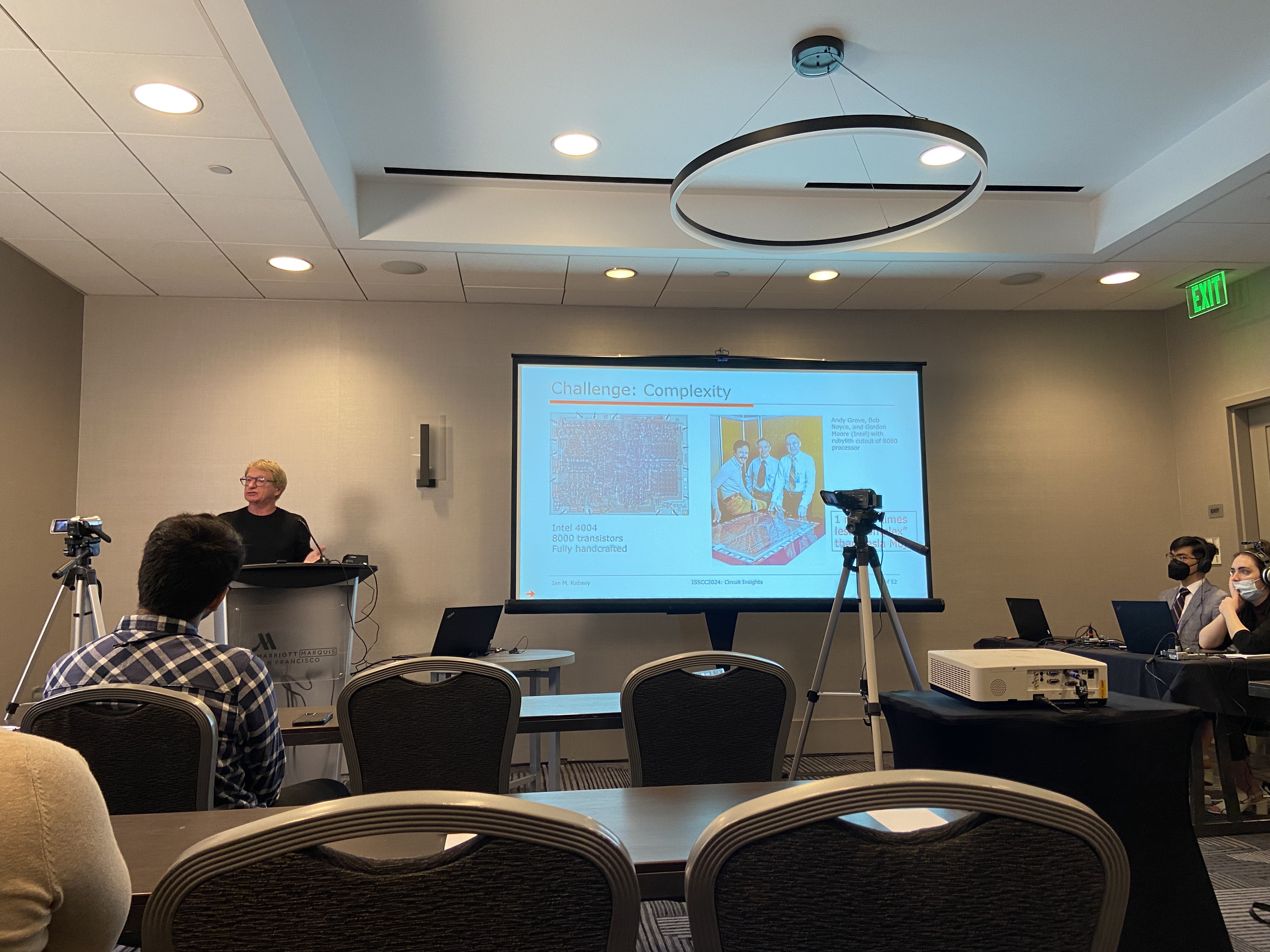
Complexity
- Intel 4004
- SPICE citcuit simulation
- Design methodology
- Verification
- Design automation
Design Methodology
- Improve productivity
- Raising abstraction level
- Design Rules Check (DRC)
- $ \lambda $-based designs rules
- CIF(Caltech Intermediate Form) language
- Connecting Fabs and Designers
- VLSI design tools
- $ \lambda $-based designs rules
- Standrd Cells
- layouts
- netlists
- automatic PNR
- RTL level
- RTL languages: VHDL and Verilog
- Structural and Behavioural level description
- Logic Synthesis
- Reuse
- Parameterized blocks
- systemverilog
- scripting language drived designs
- risc-v processors
- modern soc
- ai design tools and ai designing methodologies
- chip designs chips
Q: transistor level abstraction
R: cost of time and effort
Q: more regeneration-able substrates
R: neurons? quantums?
Q: would ai designing chips enter into problems?
R: ai designs might not be deterministic but statistical, do we need the deterministism? could we gain from the randomness? (blackbox, explanable, predictable)
Q: after manufacturing, how we could mitigate false results?
R: error correction mechanism, redundancy modules?
Q: moore’s law? the next breakthrough for future digital chips?
R: scaling has stopped; finfets, increasing density, cfet(pmos over nmos), 3d dimensional, flash memory, cmos2.0, neuromorphic
Cmos circuits for biomedical applications
Carolina Mora Lopez
human body and complexity
bioelectronics
interface with human body
- sense: getting the information from bio-electric signals
- This talk will be targeting on
- Actuate: Drive a certain organ
- Non-toxic, human-body compatible
- A research topic of material science
Biomedical Sensing
- Electrical
- Wearable sensors
- Chemical
- Optical
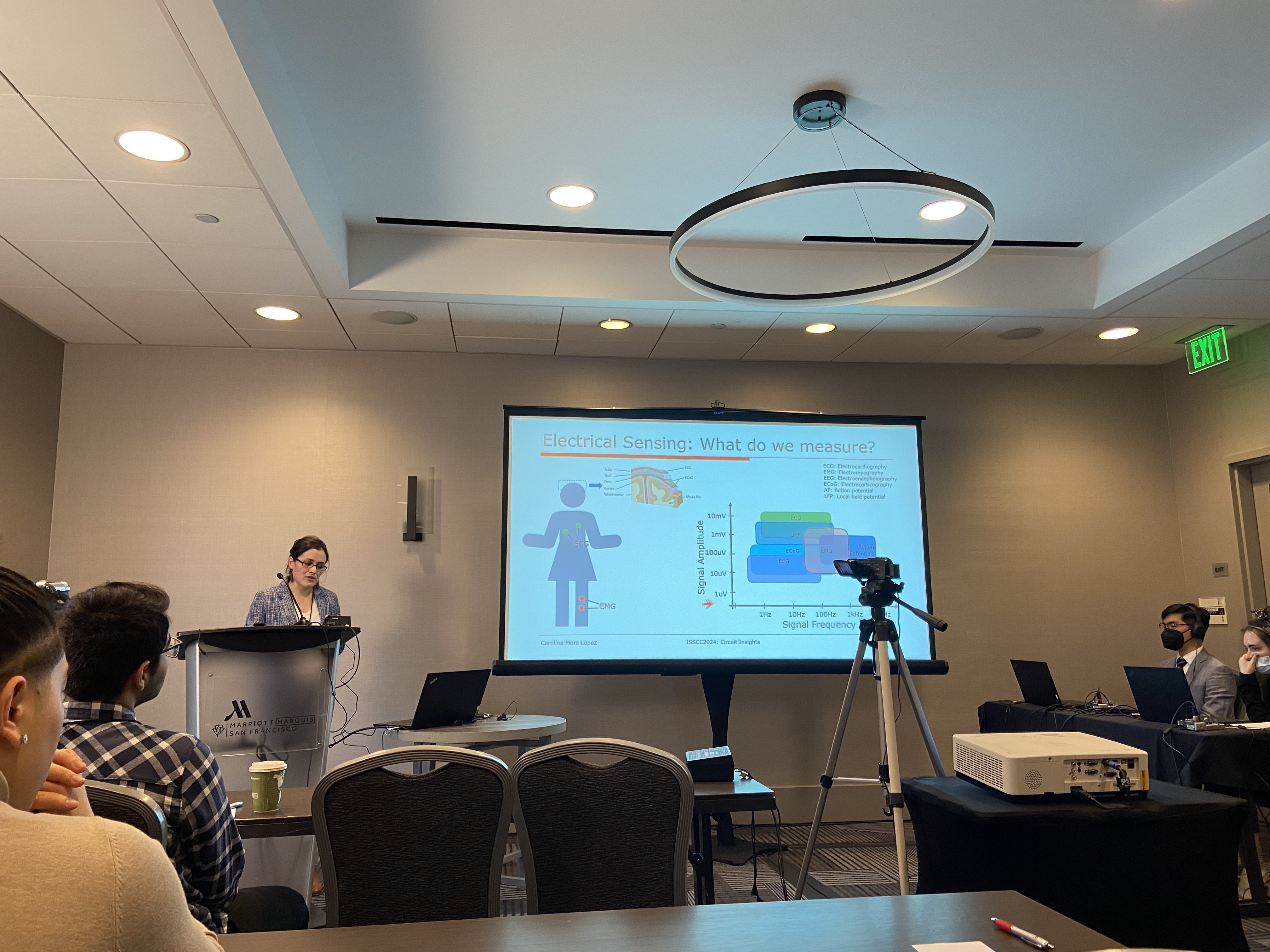
Electrical Sensing
- ECG: Electrocardiography
- EMG: Electromyography
- EEG: Electroencephalography
- ECoG: Electrocorticography
- AP: Action Potential
- LFP: Local Field Potential
Electrical Noise
Noise is defined as unwanted disturbance in an electrical signal
- Thermal Noise:
- Flicker Noise(1/f noise):
- All active devices suffer from
- Imperfections in crystalline structures of semiconductors
- Also called pink noise
- Noise Spectrum
- Corner frequency
- At low frequencies, 1/f noise dominates
- At high frequencies, thermal noise dominates
- Biopotential signals are low-frequency signals
- Affected by Thermal & Flicker noise
- Scenario case study: Amplifier input referred noise
- Input signal level: to
- Design tradeoffs:
- Noise, area and power
Interface with Biology
- Cell exerts electro-chemical reactions
- Inserting electrodes for electrical amplification and signal processing
- Electrode-Electrolyte Interface
- Electrode model as a resistor, in series with a RC parallel, in series with a voltage source
- Half-cell potential for the voltage source
Electrode DC offset (EDO)
- Different materials have different EDO values
- Electrode Impedance Magnitude
- High in low frequencies, low in high frequencies
- Electrode impedance and input impedance of the amplifier affect the amplifier input voltage by a voltage divider.
- Achieving a high impedance in AC.
- is usually a DC signal
- will be amplified
- should be rejected
- Removing EDO
- High pass filter
- Challenges: low frequency as low as 1Hz
- RC filter, differentiator
- AC coupled capacitor allows the input signals to be controlled within a DC range
- pF capacitor allows $> 100G\Omega $
- Low pass filter feed to the minus terminal to cancel
- EDO directly applied to the input, AMP needs to be able to deal with the offset
- EDO can’t be predicted well
- EDO directly applied to the input, AMP needs to be able to deal with the offset
- Low pass filter for the feedback for rejection purposes
- Highest input impedance
ELectrode Impedance
- ,
- Chopping input impedance - Achieving high input impedance
Biopotential Amplifier General Metrics
- Low noise
- EDO Rejection
- High input impedance
- Application Specific Requirements
- Small area
- Low power
- Good linearity
- Low input leakage
Q: How to mitigate DC offset?
C: Metal Capacitors
Q: BJT as compared to CMOS?
C: Low input leakage, BJT tends to have input current
Complete Biopotential Readout Circuit Architecture
- Recording Electrode / Reference Electrode
- LNA
- Filter
- Programmable Gain Amp
- ADC
- Resolution of the ADC: How many bits do we need to quantize the signal?
- Quantization noise is not significant
- Don’t want overdesign -> becomes expensive
- Power and Area constraints
- make the digital backend complex as well
LNA
- Negative Feedback loop diff amp
- AC-coupling
- High input impedance
- Low power
- How to implement ?
- Example: sheet resistance
- Pseudo-Ressistors
- Diode-connected MOS biased in cut-off
- is large for small
- Equivalent resistance value
- small area
- non-linear
- temperature dependent
- Pseudo-Ressistors
Differential Amplifiers
- Diff pair with active load, simple 5T OTA
- PMOS has lower Flicker noise for the input pair
- Diff pair and active load mosfets contribute to noise
- Noise is dominated by PMOS input pairs
- Achieving low-noise requires:
- Large for PMOS input pairs
- Small for NMOS active loads
Multi-Channel Readout
Multiple channel readouts can enable high-density sensing
Neural Readout ASIC
- Neuro-probe
- Brain behaviors
- Time-division multiplexing
- Needles
Q: The future of implantable devices?
C: Already happening, medicine already applied
Q: How to mitigate the noise?
C: With AI? Edge computing
Q: Battery and power
C: Wireless charging, inductive charging, low power all digital etc
Lunch networking
I didn’t take photos during lunch sessions but chatting with other grad students is fun and insightful.
Photos for the event:
The Basics of Radio Frequency(RF) Circuits
Hossein Hashemi
EM waves
-
Maxwell’s equations
-
EM waves are solutions to Maxwell’s equations
-
Time varying electric field and magnetic fields
- Vacuum, Air, Liquids, Solid objects
-
Propagation Delay
-
In the air, EM wave speed is the speed of light
-
Propagation delay
- Bluetooth Earbuds: 2m <=> 6ns
- Cellphone to Base Station: 1km <=>
- Earth to International Space Station: 400km <=> 1.3ms
- Earth to Mars: 1e8 km <=> 5.5 minutes
-
Wavelength
Application Frequency Wavelength FM Radio 100Mhz 3m Bluetooth 2.4GHz 12.5cm Full Body Scanner at Airports 30GHz 1cm Automative Radar 77GHz 4mm -
Radiofrencies:
- Optical:
- X-ray:
-
-
RF Circuit applications
- phones, wifi, bluetooth, radar, satellite communication, GPS, TV, Radio, Microwave ovens, RFID, NFC, etc
Modulation
- AM
- PM
- Carrier, Information, Modulator
- Demodulation
- Extract the information from the carrier
Generic Radiofrequency System
- TX
- Information
- Modulator
- RX
- Demodulator
- Information
TX and RX Circuit Architecture
- TX
- and
- Fourier Orthogonal Pairs
- LO and Mixer
- Power Amplifier
- Antenna
- and
- RX
- Bandpass Filer
- LNA
- Mixer and LO
- Low Pass Filter
- and
Passive Components
- Resistors
- Capacitors
- Inductors
- Low Pass Filter - RC circuit
Magnitude:
Passive Component Combinations
- Series LC Resonator tank
A frequency gives short circuit
Other frequencies give open circuit
- Parallel LC Resonator tank
A frequency gives open circuit(Infinite impedance!)
Other frequencies give short circuit
Filters
-
Bandpass Filters
- LC series in series with the load resistor
- LC parallel in parallel with the load resistor
-
Ladder Bandpass Filters
- Sharp Filters, high Quality Factor
RF Amplifiers
- OpAmps can’t be used for high frequencies; attennuation
- Single 1T amplifier
- Parasitic capacitance
- Always present creates a low impedance path at high frequencies
- Creating an inductor so that to form a resonator
- Bandpass behavior
- Parasitic capacitance
RF Power Amplifiers
- Can’t have high power, burn the circuit
- Transformers
- Transformers are loseless
- Impedance Transformer
RF Oscillators
- Cellphones have to generate multiple band signals
- LC Oscillators
- Energy is stored in the inductor and capacitor
- Inductors have none-infinite q factor, creating a lossy component
- Underdamping response
- Active Circuit
- Inject the lose energy back to the tank
- Self-sustained oscillators
- Crossed-coupled pair
- Colpitts Oscillator
- Hartley Oscillator
- Clapp Oscillator
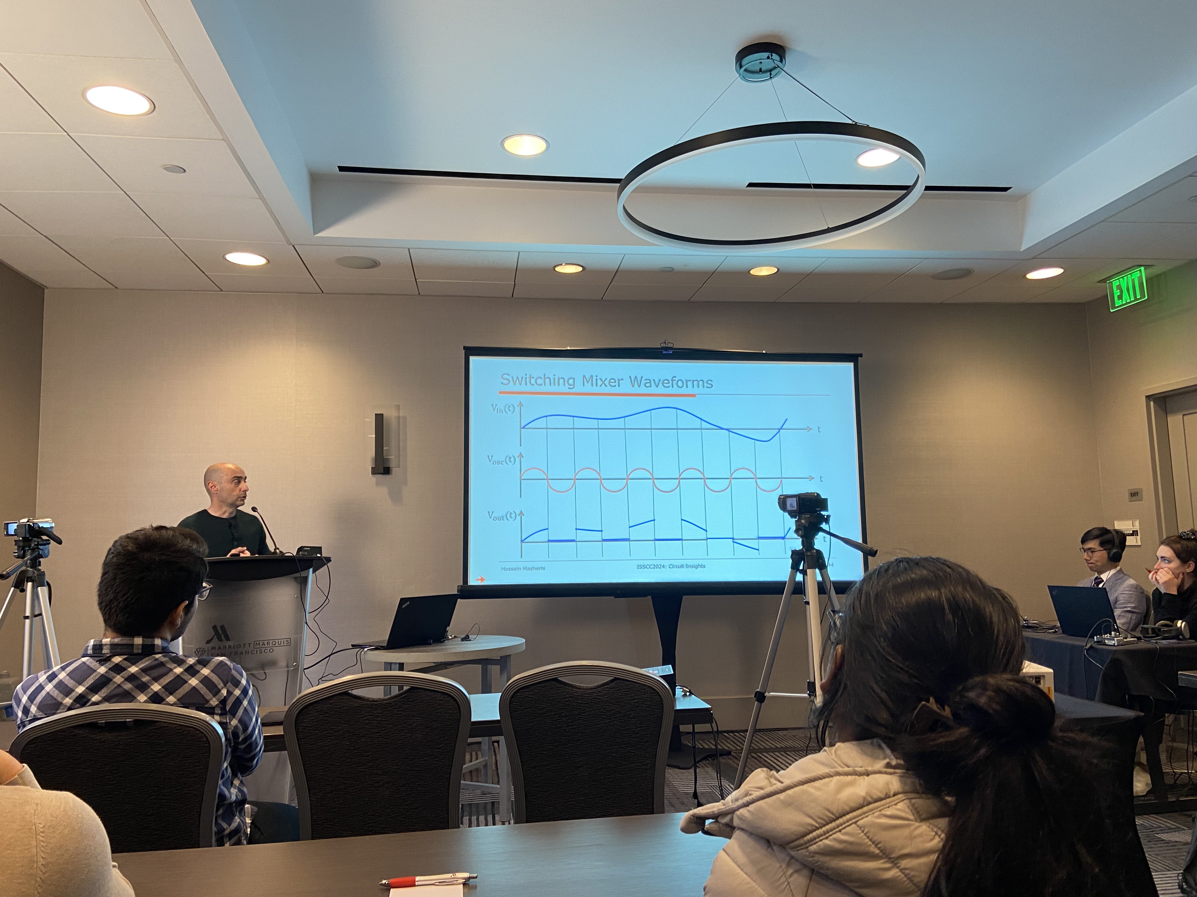
RF Mixers
- An LTI system cannot multiply two signals
- Switch doing the trick
- Multiplying with a square wave
- Fourier expansion
- Filtering using a band pass filter for unwanted higher order signals
Non-Linearities
Q: Why higher frequency?
H: Still possible, but require low wavelength
Q: Superheterodyne Receiver, switch cap, popular topologies
H: Other ways of mixing, wide-application scope
Q: Modulation techniques
H: Modulator includes the LO, Mixer and Summer, Carries is the LO
Q: How to add two signals?
H: OpAmps, KCL
The Basics of Silicon-Photonic Circuits
Sudip Shekhar
IC technologies for photonics
- IC technology roadmap
- CMOS: 1980s
- RF-CMOS: 1990s
- CMOS SOI: 2010s
- Silicon Photonics CMOS SOI starts from 2010s(Silicon On Insulator, SOI)
- Improved performance: speed, latency, parallelism
- Miniaturize discrete or bulky components
CMOS Strengths and Weaknesses
- Strengths
- Providing gain
- Switching
- Generating clock frequencies up to 100s of GHz
- Realizing complex functionalities
- Limitations
- Driving high-speed data from one chip to another over long distances, due to Cu loss
- Generating 100s of THz signal
- Interacting (sensing, detecting) with different particles and waves
Silicon Photonics
- Complelment electronics: speed, latency, parallelism
- Transceivers, Switches
- Miniaturize discrete or bulky optics
- LIDAR
- Filters
- Oscillators
- Enable new applications
- BioSensing
- Quantum Computing
Datacenters
- Pluggable modules
- Mellanox Infiniband light fiber cables
Electrical I/O Channel Loss
ISI, Inter-Symbol Interference
- Loss increases at higher data rates
- Loss increases with length of interconnect
- Equalizer helps but consumes power
- Attenuation, and low pass behavior
Optical Fiber
- Low loss
- Low frequency-dependent loss
- Wavelength-division multiplexing
- Different colors of light can be linearly added
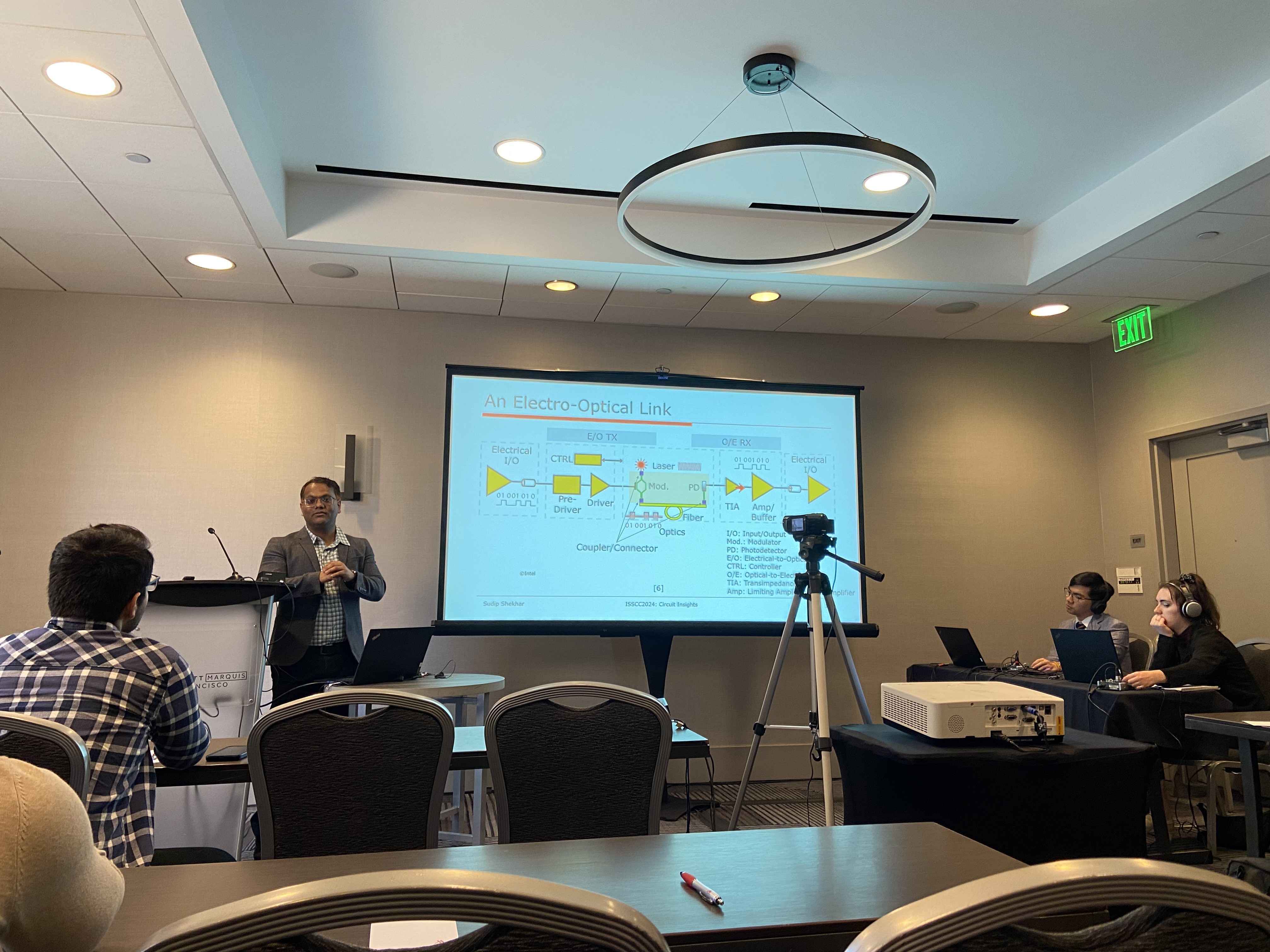
Electro-Optical Link
- Coupler and Connector to modulate the light information
- Photodetector(PD) to convert light to electrical signal
- Drivers, amplifiers
- Control the frequency. Lights tend to have super large frequency and small wavelength
- TIA: Transimpedance Amplifier
Q: Asynchronous communication in silicon photonic links?
Q: Multipath?
S: single mode fiber, getting rid of the question
Q: Key encoding(PAM modulation)
Q: Is the modulator controlled by a clock?
- SOI CMOS process
Photonics links path
- Lasers, waveguides, combiners, couplers, PD
- Si in between SiO2, total internal reflection
- Waveguide bends: to be avoided
- Operating wavelength: 1550nm and 1310nm
- Fiber-to-Waveguide couplers
- Grating couplers
- Edge couplers
- Splitter
Photodetector
- Produce current from incident photons
- When photons with power P are incident on a PD, the current produced is
Silicon Photonic Circuits
- Mach-Zehnder Interfereometer
- Phase shifter
- Modulator
- Switch
- set the phase shift for constructively interference and destructively interference
- How do we do the phase shifter?
- Changing the phase of the light
- Refractive index, phase, attenuation
- Optical Path Difference
- Thermal Phase Shifter
- Silicon
- Put a resistor next to the shifter
- High-Speed Phase Shifter
- Dope the Si rib waveguide to make a pn junction
- Apply a voltage to the pn junction, change the free-carrier concentrations
- Complex refractive index =
- Higher loss if the voltage is higher
Mach-Zehnder Interfereometer
- Switching just like a
MZM Electro-Optical Bandwidth
- RC parasitics
Silicon Photonic Circuits
Q: PAM modulation, equalizer?
S: Synchronization problems can’t be removed by optical links
Q: Shot noise in the modulator?
Q: Do I have to worry about diffraction?
S: Eliminate diffraction. Not a problem
Q: What if I want diffraction?
S: Couple light into a chip, (grating coupler),
Q: Clock recovery
S: phase noise, amplitude modulation - not such a concern, AM radio error
Q: wavelength division multiplexing
S: Frequency-division multiplexing, in copper would have crosstalks - in optical fiber, the crosstalk is very small.
There will be a tutorial session on Sunday and paper presentations on Monday onwards. I will be attending the tutorial session and taking notes as well.
ISSCC Tutorials, Feb 18th 2024
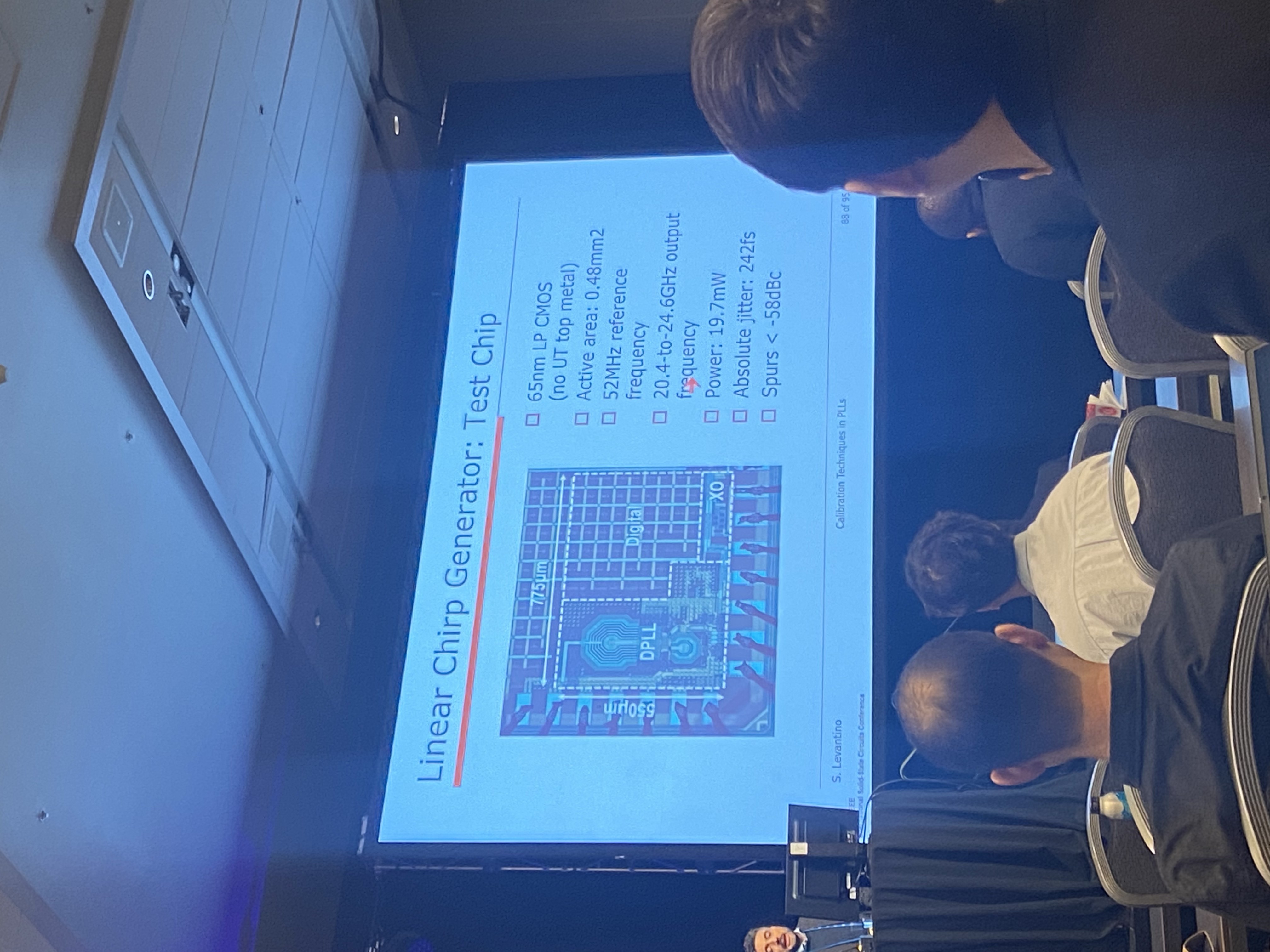
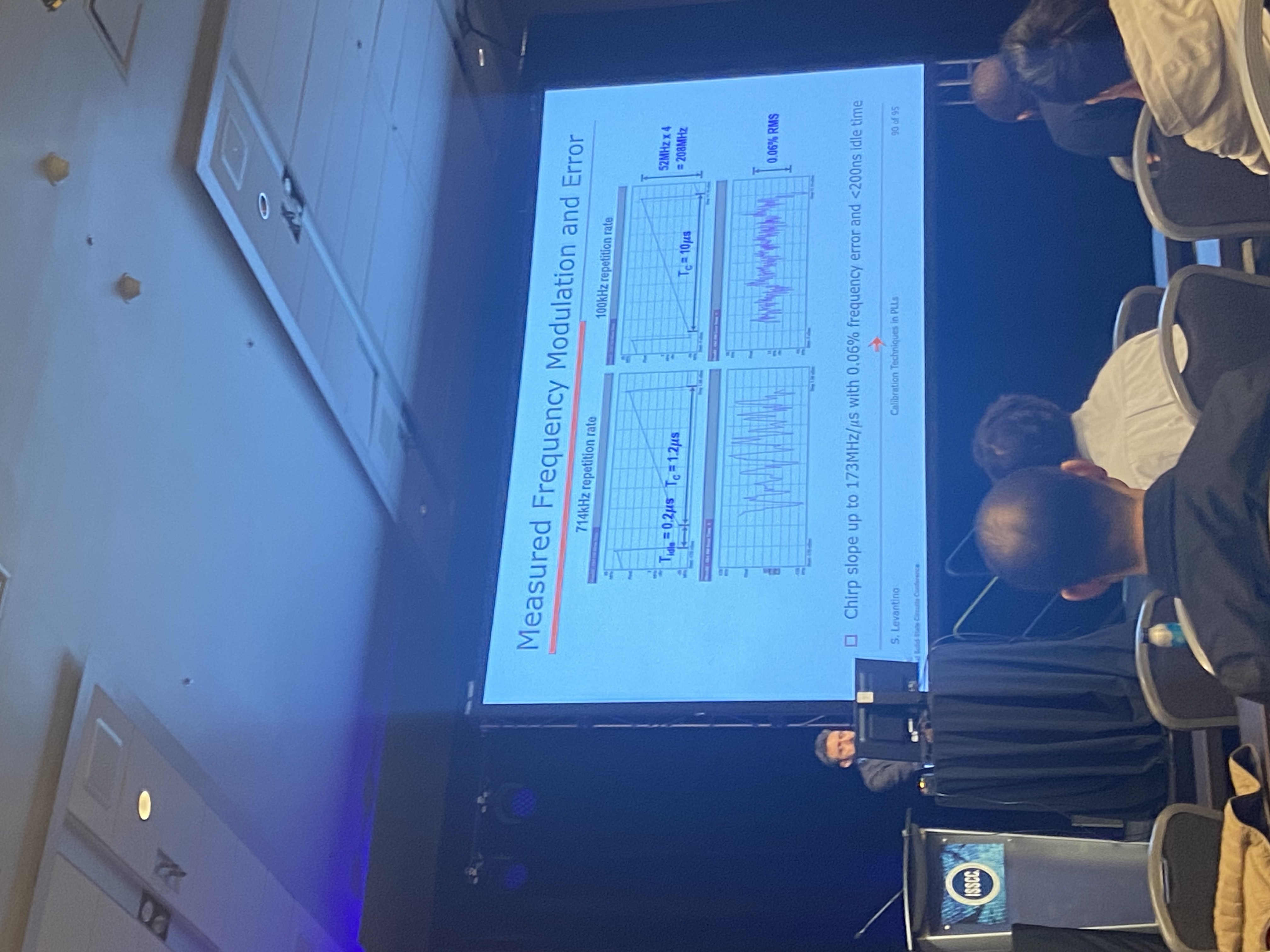
Calibration Techniques in PLLs
Salvatore Levantino
General Concepts of PLL
- Architecture
- Phase Detector
- Analog Loop Filter
- VCO
- Tracking the phase
- Divide by Integer N
- Digital counter (frequency divider) in feedback
-
- Frequency divider has a modulus control
- modulator to dither MC to achieve frequency division
- DAC
- Suffer from quantization error, phase error is an integral of time
- Frequency spurs
- Calibrated DAC to mitigate Noise
- The DAC requires calibration to match the gain of the divider/PD cascade
Common Applications of PLLs
- Clock Multiplication
- Frequency synthesis
- Skew suppresion
- Clock Recovery
- FM modulation/demodulation
Frequency Synthesis
- Complex QAM schemes at mmW require low LO phase noise
Implementation PLLs
Analog charge-pump PLL
- Phase-frequency detector(PFD)
- depend of the phase difference
- using a filter for analog filtering purposes
- Area and power doesn’t allow for CMOS progression
Digital PLLs
- DCO
- TDC, Time-to-Digital Converter
- delay line structure based on FFs
- TDC is a digital circuit
- Records the error with respect to the reference clock
- Thermal metered code
- DCO: LC oscillation using digitally coded capacitance.
- Digital loop filter
- PI control; proportional and integral
- FIR filter
- Pros and cons
- digital filter replaces the bulky ones
- charge pump is absent(less power, power, area)
- More friendly to calibration
- TDC and DCO contribute to noise
Cancellation of $ \Delta \Sigma $ Quantization Noise
- The $ \Delta \Sigma $ noise can actually be cancelled
Adaptive Filtering
- Adaptive filtering
- Linear Estimation
- Steepest Descent Algorithm
- Cost function
- Convergence and Stability is dependent of steep size $\mu $
- Stochastic Gradient Algorithms: LMS case(least mean square)
- Classes of Adaptive filtering
- Interference cancellation
- Inverse Modelling
- Equalize the response, cancel the effect of the channel(likely low pass)
- Channel equalization
- System Identification
- Mimics the behavior of an unknown system
- Linear Prediction
Calibration Examples
- Applications
- Quantization noise cancelaltion(interference cancellation)
- Automatic bandwidth control(System identification)
- Linear modulation(Inverse modeling)
- LMS loop
- Measure error, integrate, substract
- TDC nonlinearity
- Phase Interpolation to reduce TDC range
- PI mismatches
- such mismatches in the PI phases produces spurious tones
- PI has to be linear as well, creating same stpes
- Multi-Pase LMS Adaptive Filter
- DTC-Assisted Bang-Bang Digital PLL
- Only vary by 1 bit
- Power is reduced due to the Bang-Bang TDC
- DTC-Assisted Sampling PLL
- FoM: Jitter times power, inverse proportionality
Automatic Bandwidth Control in PLLs
- Loop Gain Sensitivity
- Loop Gain Normalization
- Adaptive filtering stabilize the phase noise response
- Bandwidth control
Linearized FM Modulation of a PLL
-
Direct FM Modulation
- Pros: low Power, fine resolution, linearity
- Cons: slow frequency switching, fractional spurs, modulation rate limited by loop BW
-
Two-point injection
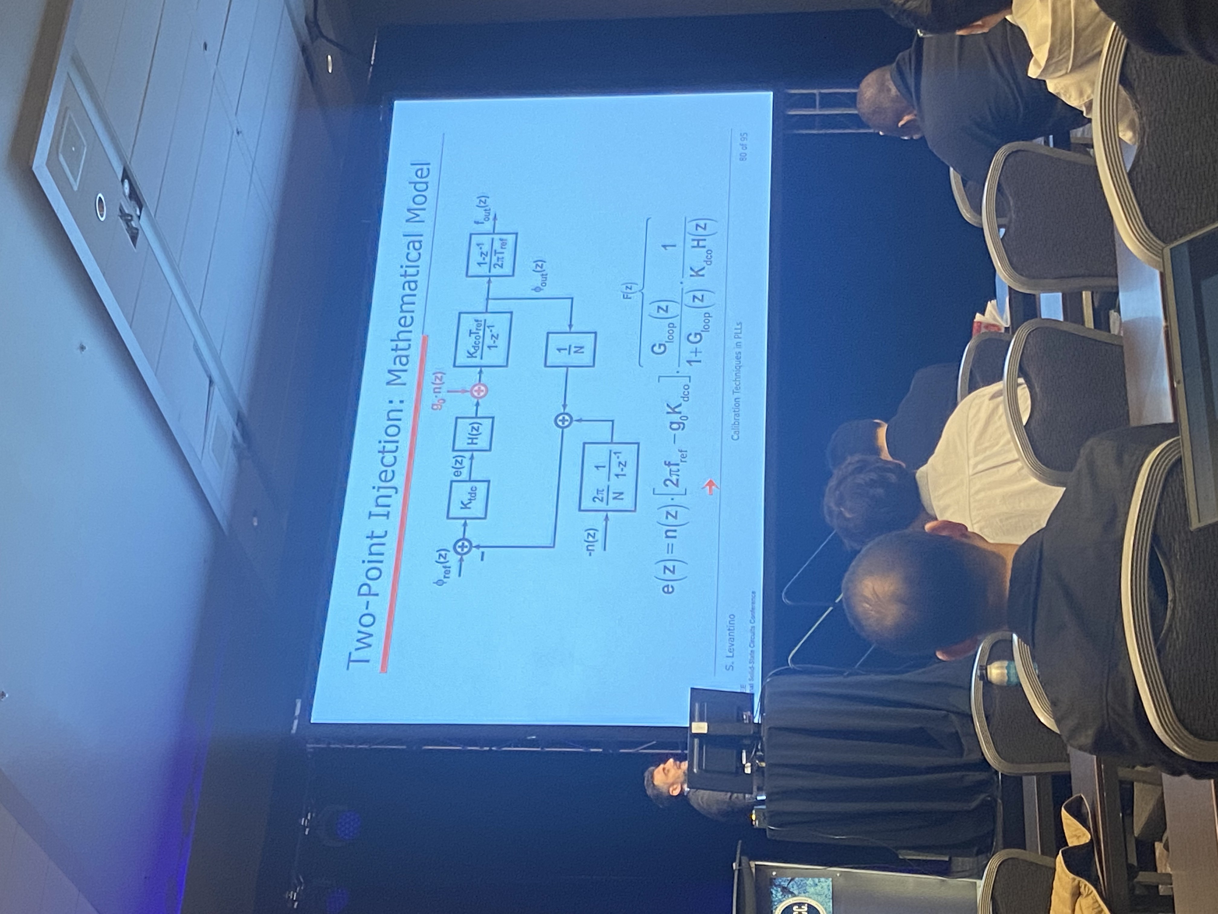
- All-pass transfer function if the two gains match
- Enables fast direct-FM modulation of a PLL
- Requires gain calibration
- Adapative filtering techniques applied
- Gain imbalance correction
- Integration to produce phase
- Produce error, integrate, produce new gain
- Integration to produce phase
- DCO nonlinearity
- DCO gain differs at the edges of tuning range
- Intra-band nonlinearity from capacitor mistmatches
- Chip modulation would contain frequency errors
-
Adpative DPD Algorithm
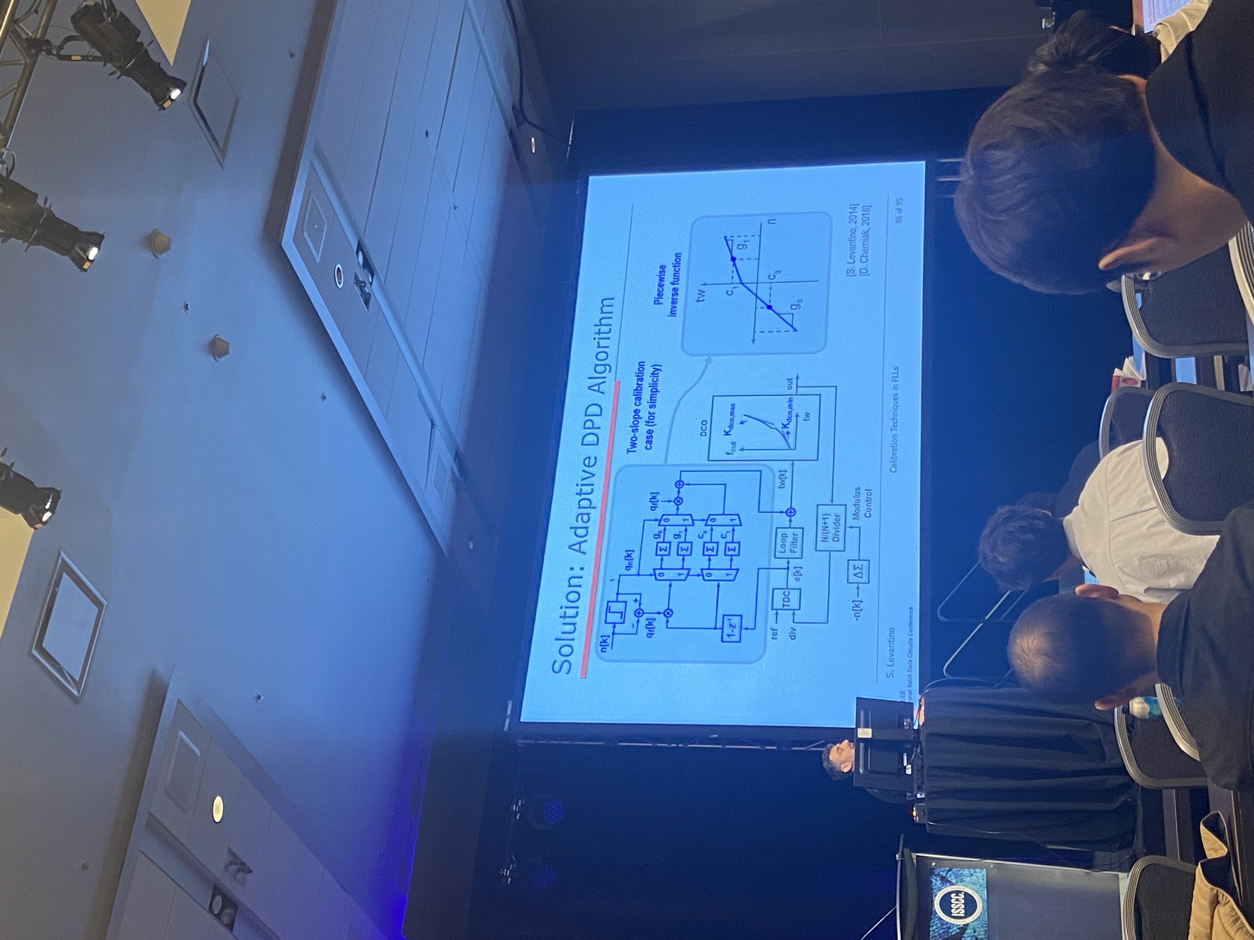
- Digital Predistortion Algorithm
- Estimate two different gains, and compensate
- Getting two different gains using accumulators
- Frequency jump enables quick settling time
- Digital Predistortion Algorithm