This is a paraphrase of the tutorial talk by Prof. Pavan Hanumolu from UIUC on Clock and Data Recovery (CDR) basics. The talk was given at the 2015 IEEE International Conference on Solid-State Circuits (ISSCC) in San Francisco, CA.
I made some annotations to the slides. You can find the combined slides and my annotations below.
From Asynchronous Link to Synchronous Link
I discussed the implementation of the UART protocol in an ancient post. UART is an asynchronous protocol, which means that the transmitter and receiver do not share a common clock. However, since the data stream is slow enough, the receiver can sample the data stream at a rate that is close enough to the transmitter’s clock.
However, as we push the data rate higher, the sampling precision required to recover the data stream becomes more stringent. For example, at 1 Gbps, the bit period is 1 ns. If we want to sample the data stream in the middle of the bit period, we need to sample with a precision of 0.5 ns. This is not feasible with an asynchronous protocol like UART.
From an encoded data stream, it’s then interesting how we shall retrieve the clock information from the data stream. This is where Clock and Data Recovery (CDR) comes into play. CDR is a technique used to recover the clock signal from a data stream, allowing for synchronous communication even when the transmitter and receiver do not share a common clock.
CDR is used in multiple protocols, including PCIe and SATA. One advantage of using CDR is that it allows for only data streams to be sent over, thus ensuring the minimum number of wires are used (we are not building simultaneous bi-directional links, unfortunately). The system that utilizes CDR is also sometimes referred to as an “embedded clock” system.
Unlike the embedded clock system, the counterpart is usually referred to as the “forwarded clock” system, which most of the time finds its application in massively parallel links, such as die-to-die interconnects where we can amortize the cost of sending one more clock over many data lanes, which is part of my PhD research. I’ll dedicate another post to discuss the forwarded clock system in more detail, but in this post we will focus on the embedded clock system and CDR.
CDR Metrics
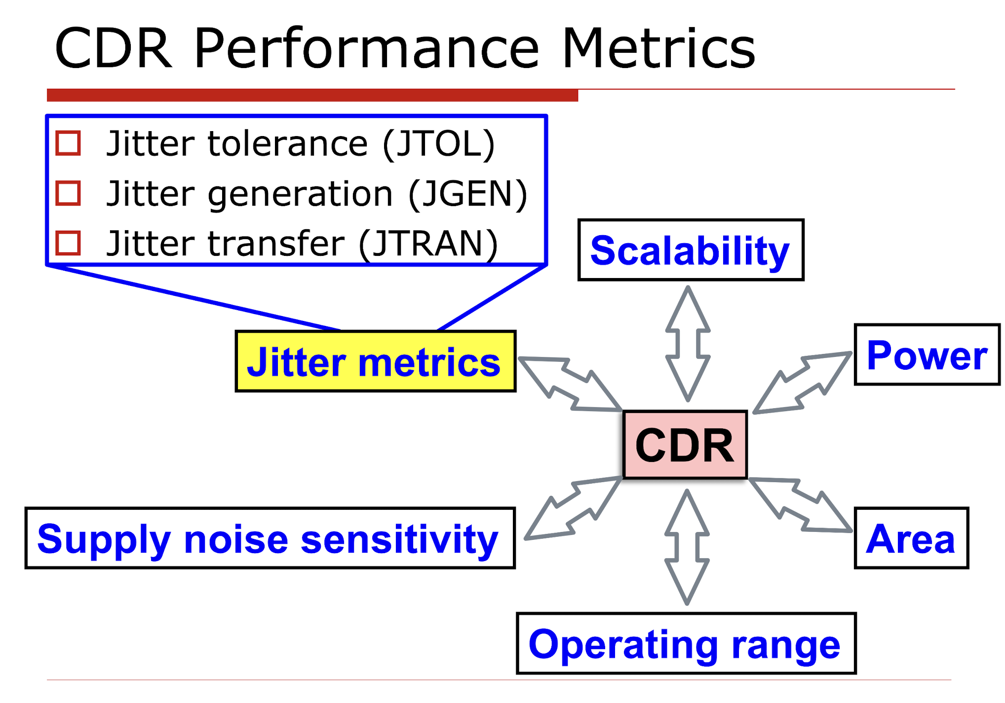
Like any other AMS system, we want to build CDR with scalability, low power, low area, high operating range, and immunity to supply noise. However, aside from all these conventional PPA (power, performance, area) metrics, there are 3 more metrics that are specific to CDR. They are:
- Jitter Tolerance: The ability of the CDR to tolerate jitter in the incoming data stream.
- Jitter Generation: The amount of jitter that the CDR adds to the recovered clock.
- Jitter Transfer: The ability of the CDR to transfer jitter from the incoming data stream to the recovered clock.
Among all these, usually jitter tolerance is the main metric that we would like to optimize for.
JTOL
Jitter Tolerance (JTOL) measures how much jitter the CDR can tolerate in the incoming data stream before a bit error is sampled. JTOL is usually measured in terms of a “JTOL mask” which looks like:
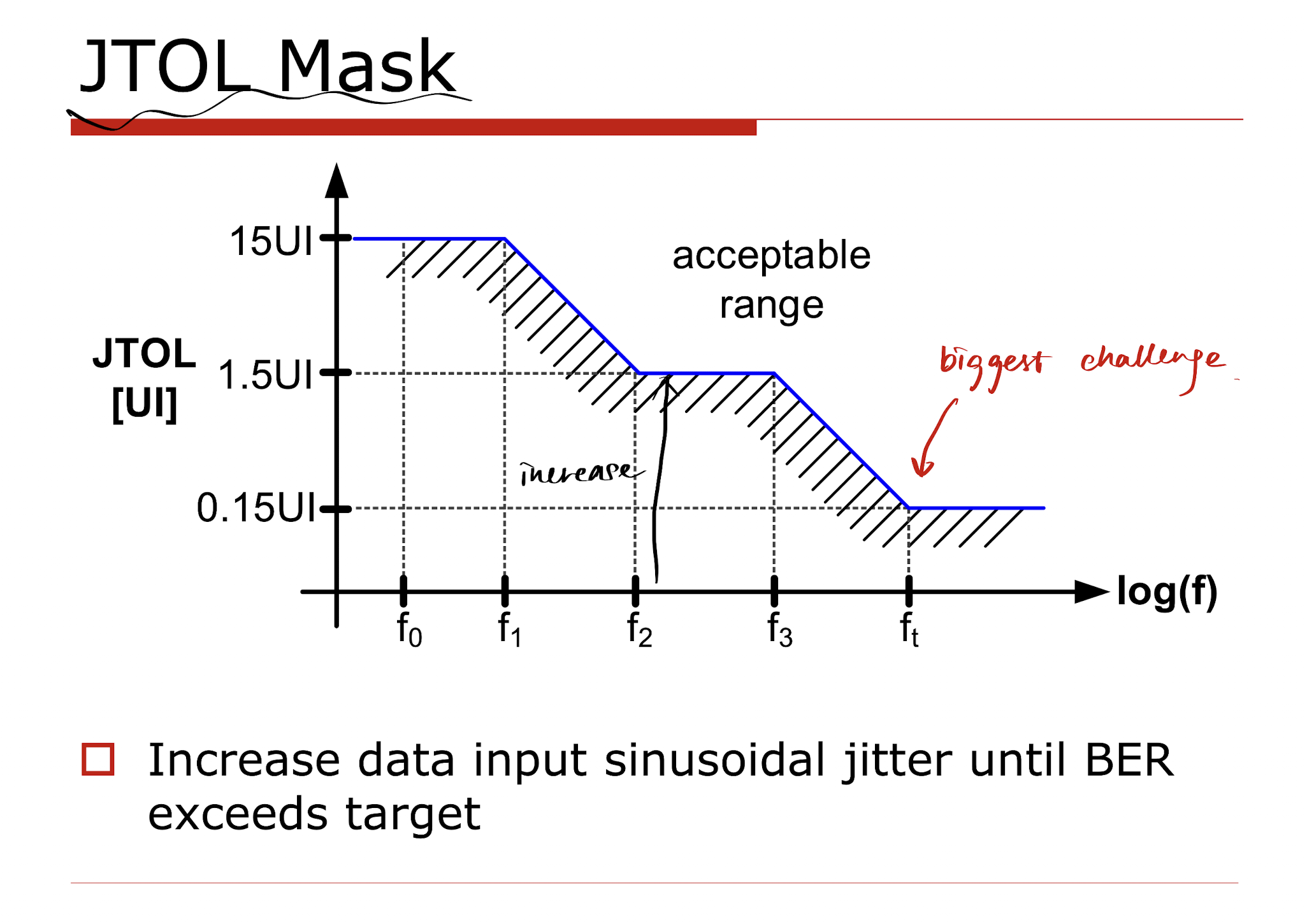
Usually a closed loop clocking system is able to track the low frequency drifting, while it fails to track the high frequency jitter. Therefore the JTOL mask is such that a CDR can usually tolerate large jitter when the jitter frequency is low, but can only tolerate small jitter when the jitter frequency is high. In actual measurements, we apply sinusoidal jitter to the incoming data stream and measure if a bit error happened, which defines the JTOL boundary. We would like the actual measured JTOL curve to be above the JTOL mask.
The JTOL mask also defines the jitter tolerance bandwidth, which we will discuss in more detail later.
JTRAN
Jitter transfer (JTRAN) measures how much jitter is transferred from the incoming data stream. This metric is sometimes a little trickier to deal with, as it’s not always good to transfer all jitter, or no jitter, to the recovered clock.
We also measure JTRAN in terms of a “JTRAN mask” which looks like:
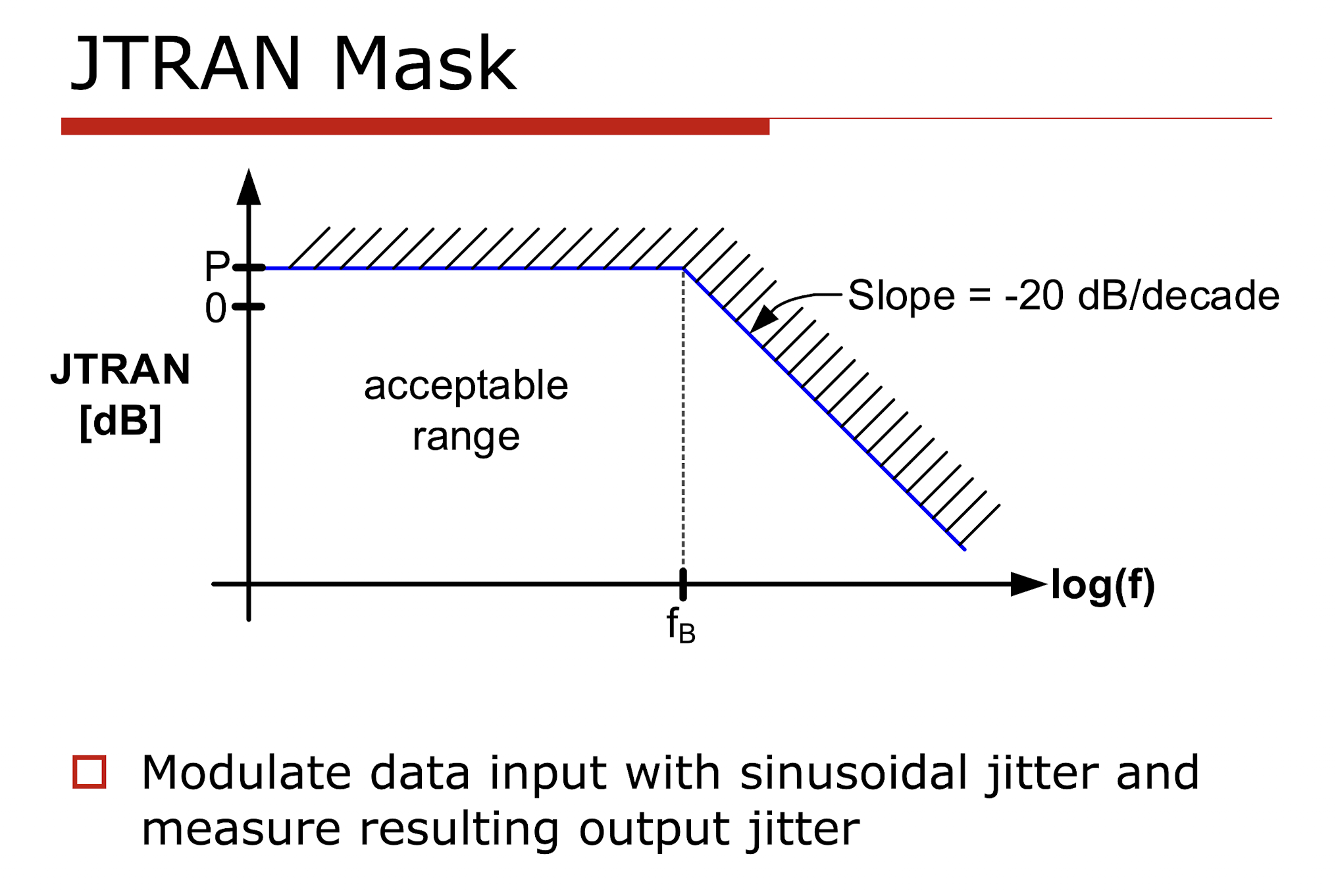
This transfer function looks a lot like a low pass filter, or in more precise terms, the reference-to-output transfer function of a closed loop PLL.
JGEN
Jitter generation is a simpler metric. Usually the smaller the jitter generation, the better. It measures how much jitter from the CDR itself is added to the recovered clock.
It’s worth noting that JGEN is not always decoupled from the input clock jitter; sometimes JGEN can be a function of the input clock jitter. The reason is that the system bandwidth can sometimes be determined by the input jitter if we have for example a BBPD whose gain is a function of the input jitter.
CDR Architectures
One can think of CDR as something that generates a clock from the incoming data stream. If the input clock drifts, the CDR also drifts. In that sense a CDR can be thought of as just a PLL. Then, why don’t we use a traditional PLL to recover the clock?
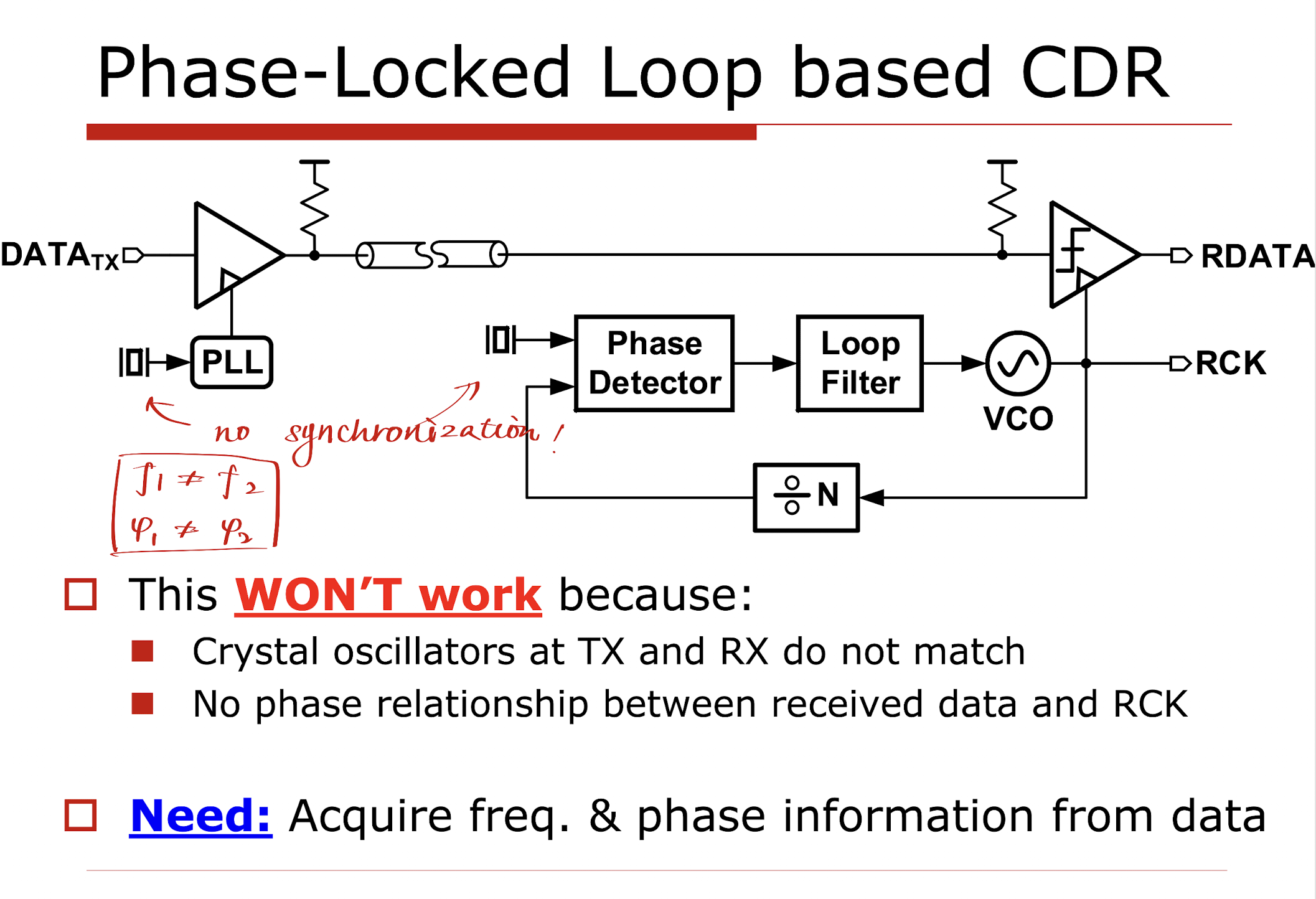
In the illustration, we have two “identical” crystal oscillators, one at the TX and the other at the RX. We use two oscillators to clock the two identical PLLs, hoping to generate two clocks that are the same. However in reality, the two crystal oscillators are not purely identical: any small ppm offset will lead to a random-walk based phase drift which can be modeled as a Brownian motion. The phase drift will accumulate over time, and the two clocks will eventually drift apart, and cause bit errors in the data stream.
It’s worth noting that if the PLL’s output clock is SUFFICIENTLY SLOW, this scheme can actually work, and we are falling back to the UART case. However, for a higher speed case, we’ll have to make sure the generated clock is based off the incoming data, instead of some other asynchronous sources. In other words:
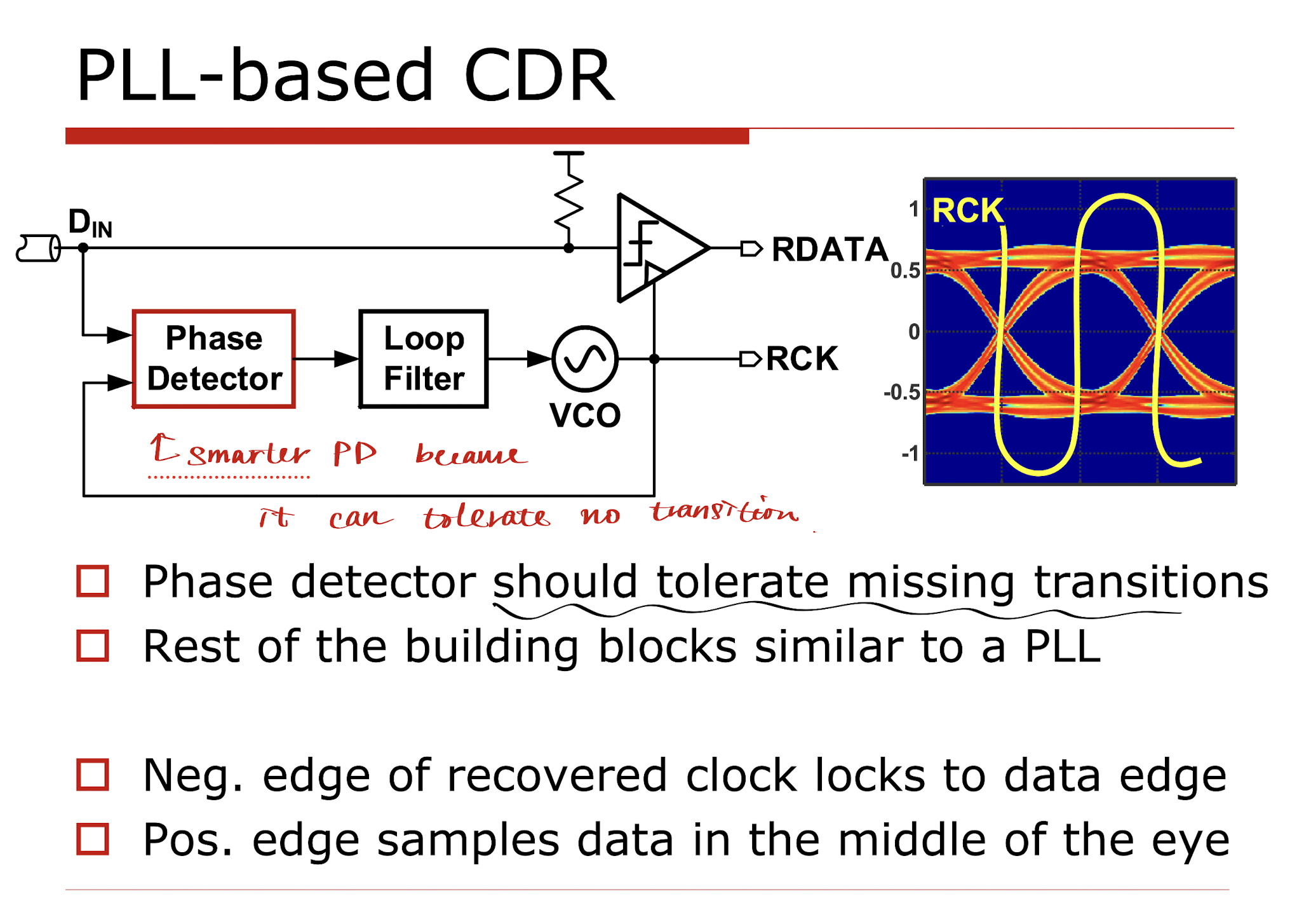
- The generated clock should compare the clock from itself with the incoming data stream.
- If there is no transition in the data, we don’t have any information about the clock, and we should not change the generated clock.
- The resulting clock should be such that the rising edge aligns to the middle of the data eye, and the falling edge aligns to the transition, if the eye is symmetric.
With all these requirements, one can see that we just need a special phase detector to tell if we are “fast” or “slow”. Indeed, the type of phase detector used will define how our CDR system behaves.
Linear CDR
Hogge PD Basics
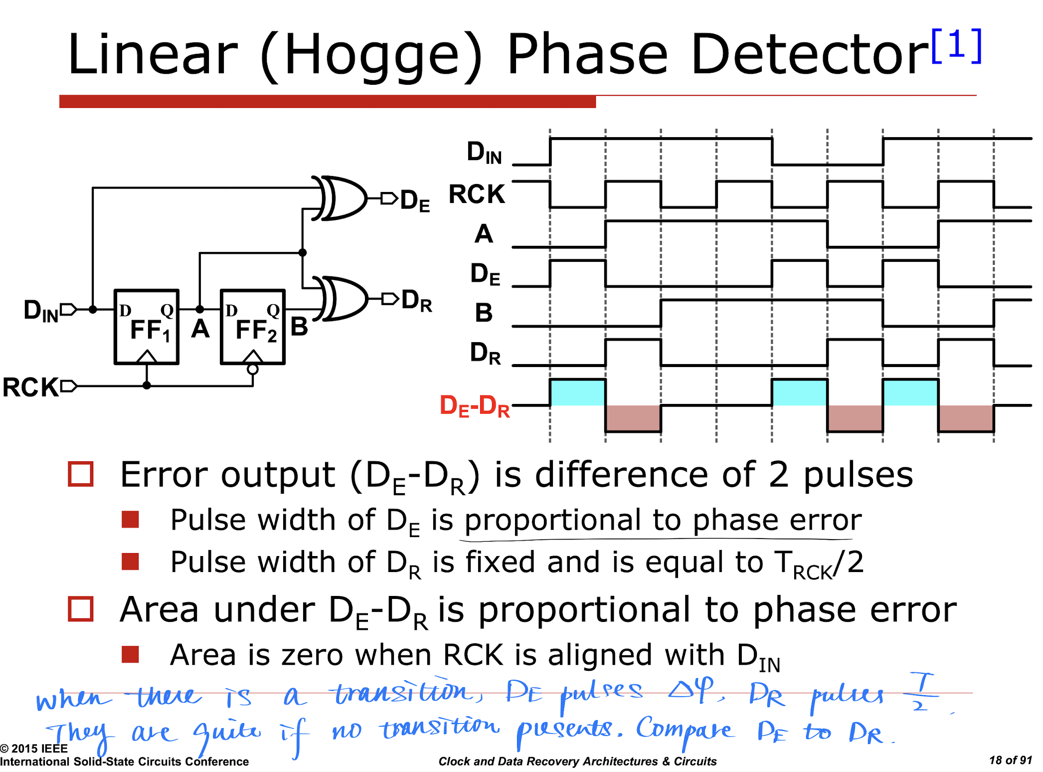
The first candidate is what is known as the “Hogge Phase Detector” published by Charles Hogge in 1985 in IEEE Transactions on Electron Devices.
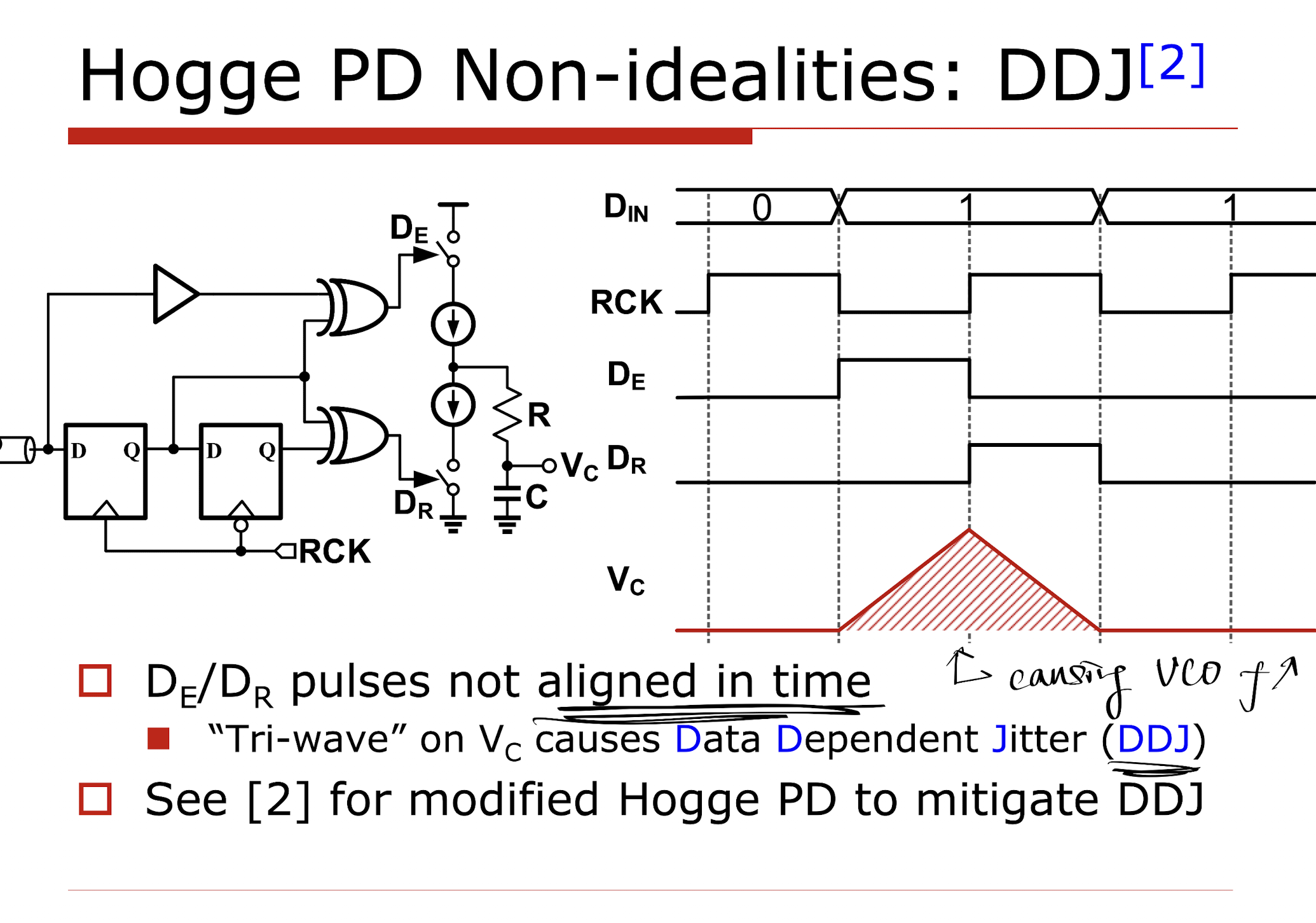
The Hogge PD is a linear phase detector, whose operating principle is to subtract the results of $D_E$ and $D_R$.
Whenever there is a transition in the data, $D_E$ will generate an up-pulse whose width is proportional to the phase difference between the generated clock and the incoming data. Right after $D_E$ falls back, $D_R$ will generate another up-pulse, but whose width will always be half of the generated clock period. Therefore, by comparing the relative width of the two pulses, we can determine if the generated clock is “fast” or “slow”.
It’s easy to post-process the output of the Hogge PD by simply using a charge-pump circuit, just like what we will do for a PFD-based PLL:
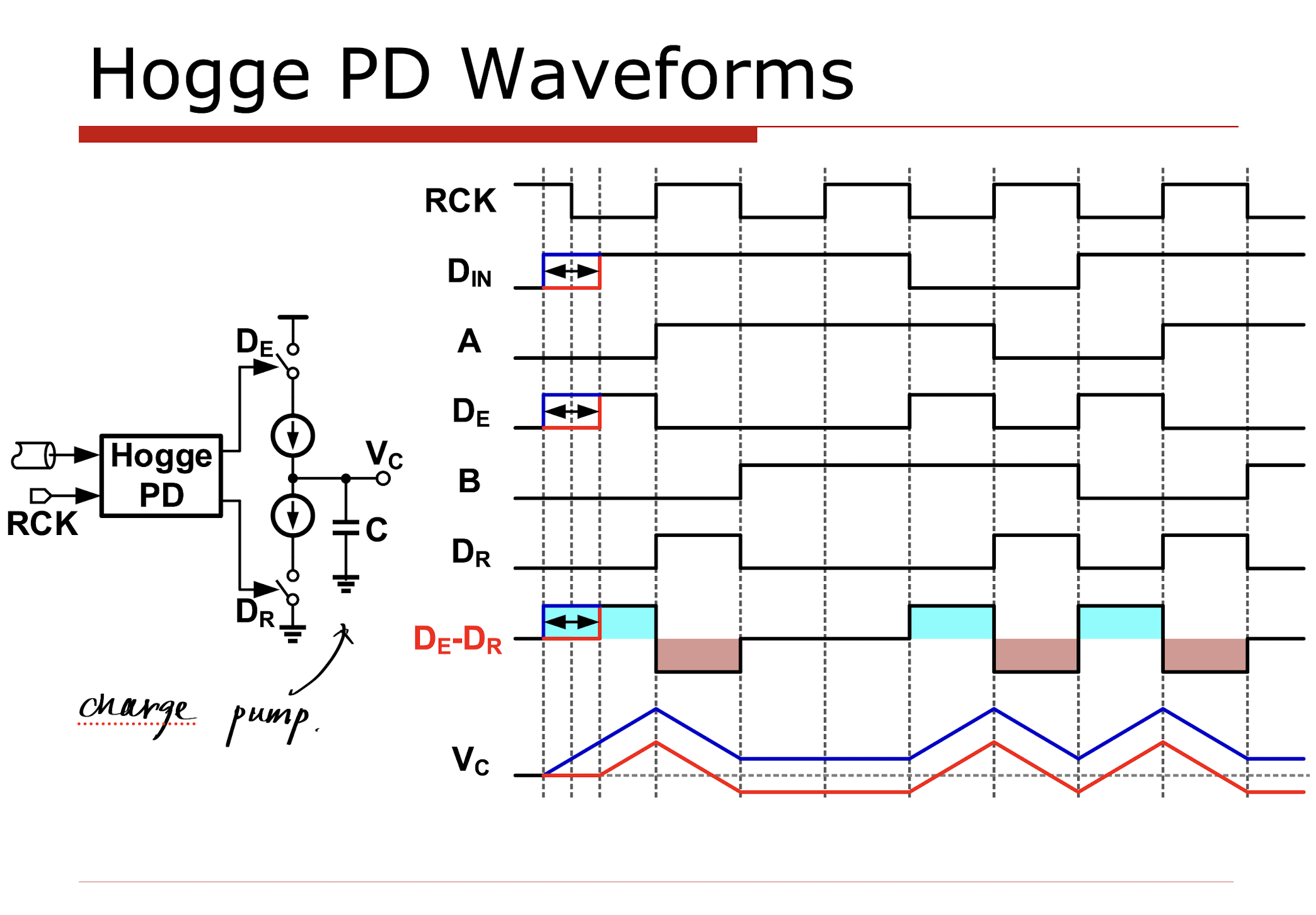
As can be seen, the resulting voltage at $V_C$ will get high if the data leads the clock edge, and low if the data lags the clock edge. This voltage can then be used to control a VCO, which will generate a clock that is aligned with the incoming data stream.
Compare Hogge PD to a PFD
Now, if we plot the transfer function of the Hogge PD, it actually behaves differently from a PFD:
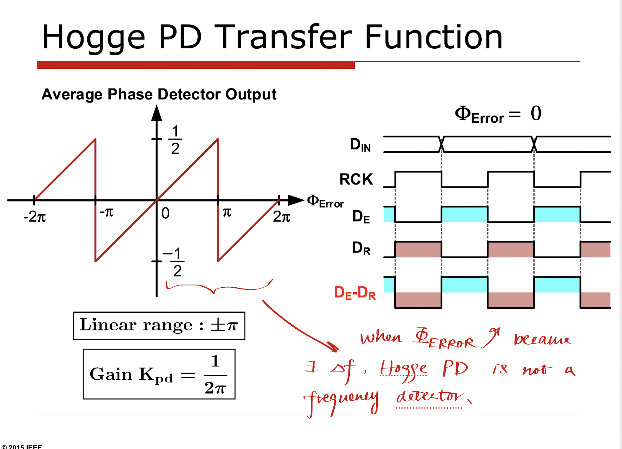
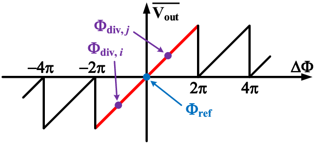
They look pretty similar within the $\pm \pi$ range, however the Hogge PD falls back to below zero when the phase difference is larger than $\pi$. However for a PFD, the output will always be positive (or 0), if the phase difference is greater than 0.
Now think about the case where, instead of a phase difference, we have a frequency difference. The former corresponds to a step response in phase (type 0), and the latter corresponds to a ramp (type 1). As we move to the right in the phase plot for the PFD, we are always seeing something positive, therefore the average value is going to be all positive. However if we do so for a Hogge PD, because of the nature of both positive and negative values, the average value will be precisely 0, which means the Hogge PD is not able to serve as a frequency detector. This will be something to keep in mind if the VCO frequency tuning range is so large that we might have a large frequency difference between the incoming data and the generated clock, causing the acquisition to fail.
CDR Loop Dynamics
Using the Hogge PD to replace the PFD in a PLL, and removing the frequency divider, we can get a CDR loop that looks like:
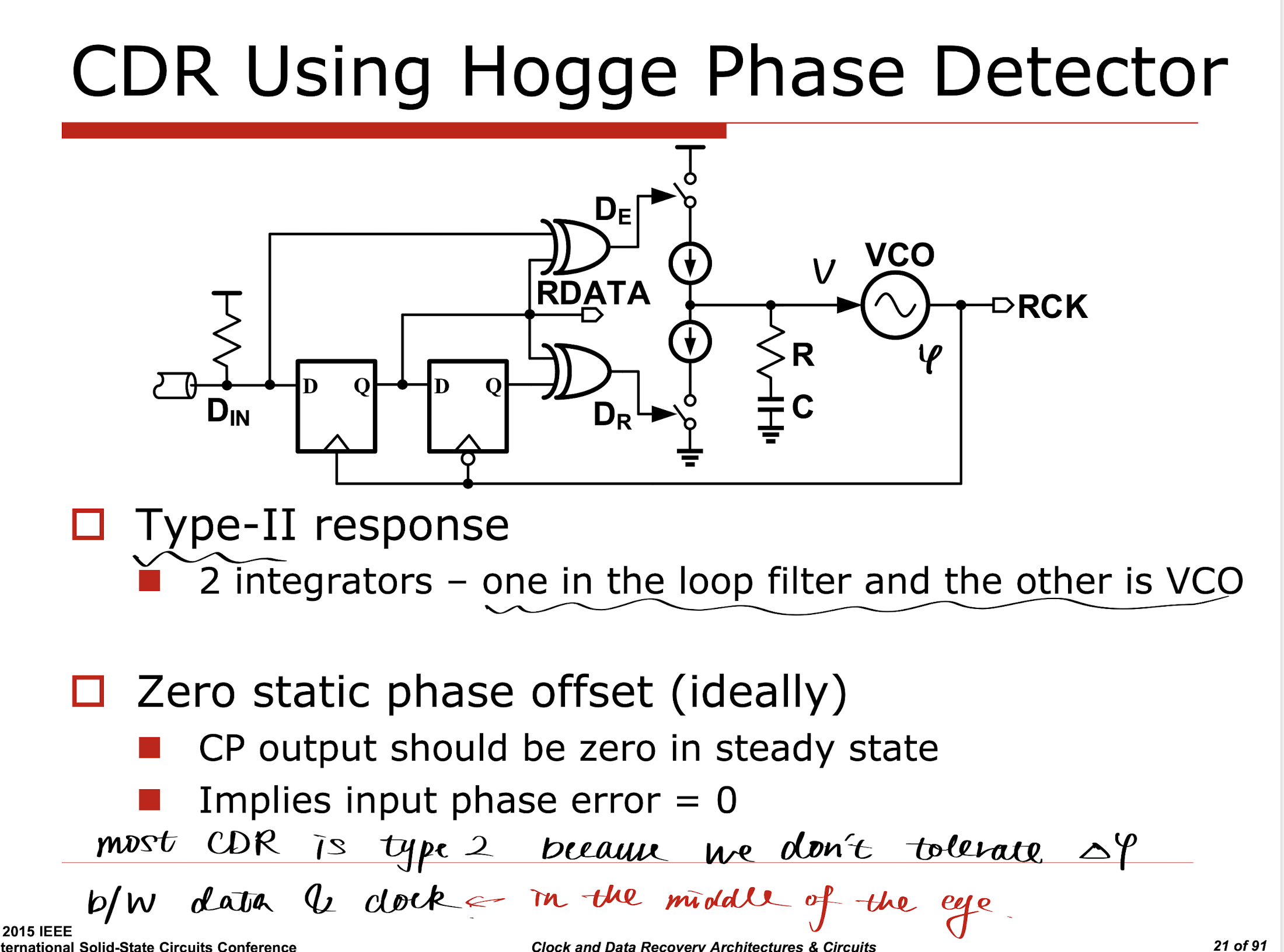
Notice that the VCO is itself an integrator because the output is phase instead of frequency. One can identify the loop as a type 2 system, which can track type 1 input well, and cancel any steady-state phase offset. This is crucial because we always want to generate a clock that’s, in the long run, sitting at the middle of the eye. This is however not necessarily the requirement if we were to implement a PLL, where we only care about the phase cleanness instead of whether it’s 100% aligned to the input clock.
With a loop that looks like above, we are now ready to perform loop analysis.
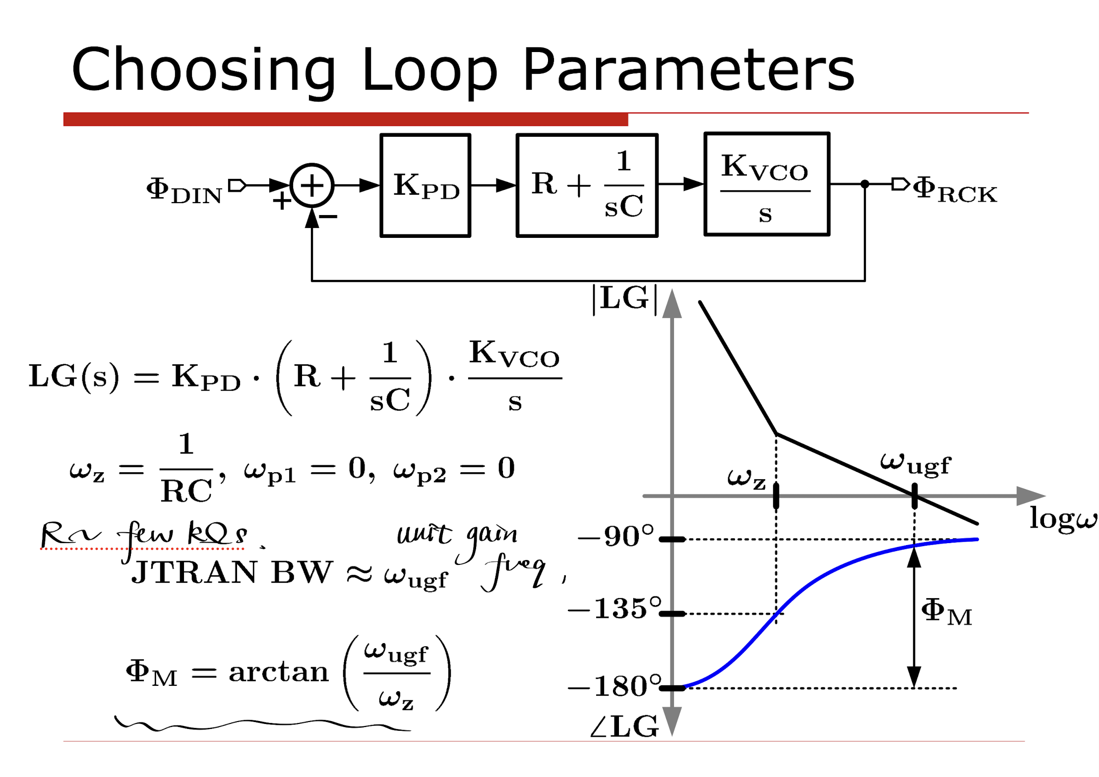
One must be careful about the gain of the PD in this case. For the Hogge PD, although we did derive the gain as $K_{PD} = \frac{1}{2 \pi}$, this is only true if the input data is always doing transitions, or sending 01010101… pattern. In real practice, the transition density of the input will render the gain of the PD to be lower than this value.
By introducing a damping resistor $R$ in the CDR loop, we ensure a positive phase margin, otherwise the double integrator system will be marginally stable. The zero created by the resistor locates at $\omega_z = \frac{1}{RC}$, and the phase margin is a function of both the loop unity gain frequency and the zero frequency:
$$ \Phi_M = \tan^{-1} \left( \frac{\omega_{ugf}}{\omega_{z}} \right) $$We are also able to derive the jitter transfer bandwidth:
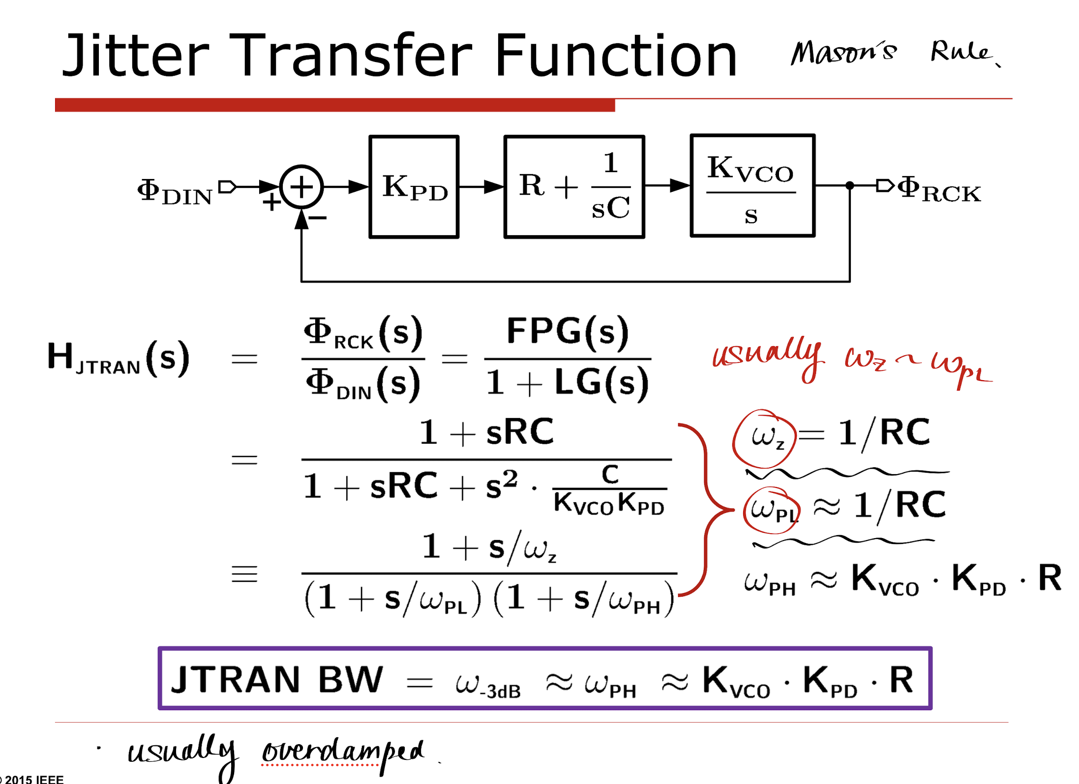
We will discuss more about how we managed to derive $\omega_{-3dB} = K_{VCO}K_{PD}R$ in the next section.
Linear CDR Drawbacks
There are a couple of drawbacks when using a linear CDR, especially when a Hogge PD is used.
Jitter Peaking
From Mason’s Gain Formula, we already derived the input-output jitter transfer function of the linear CDR loop:
$$ \frac{\phi_{out}}{\phi_{in}} = \frac{1 + sRC}{1 + sRC + s^2 \frac{C}{K_{VCO}K_{PD}}} $$We can easily identify the zero being:
$$ \omega_z = \frac{1}{RC} $$The pole locations are unfortunately not so straightforward. Prof. Behzad Razavi has a nice derivation in his book “Design of CMOS Phase Locked Loops”, chapter 8.1. It’s worth noting that the derivation is based on a type 2 PLL, but it applies exactly to the CDR loop as well here.
We try to use a generalized version of the type 2 loop and recognize the input-output transfer function as:
$$ H(s) = \frac{2\zeta \omega_n s + \omega_n^2}{s^2 + 2\zeta \omega_n s + \omega_n^2} $$We are therefore able to find the two poles:
$$ \omega_p = (-\zeta \pm \sqrt{\zeta^2 - 1})\omega_n$$- If $\zeta = 1$, we have a critically damped system, and the two poles are at $\omega_n$.
- note that in this case both poles have their magnitude larger than $\omega_z = \frac{\omega_n}{2\zeta}$.
- If $\zeta \gg 1$, we recall the following approximation: $ \sqrt{\zeta^2 - 1} \approx \zeta - \frac{1}{2\zeta} $, using which:
- $\omega_{p1} \approx (-\zeta + \zeta - \frac{1}{2\zeta})\omega_n = -\frac{\omega_n}{2\zeta} = -\omega_z$, i.e. the first pole is at the same location as the zero.
- IMPORTANT FACT: It’s still slightly larger than the zero!
- $\omega_{p2} \approx (-\zeta - \zeta + \frac{1}{2\zeta})\omega_n = -2\zeta \omega_n$, i.e. the second pole is at a much higher frequency than the zero.
If we were to plot the zero-pole locations on the Bode plot, we will be able to see a peaking produced by the first zero-pole pair:
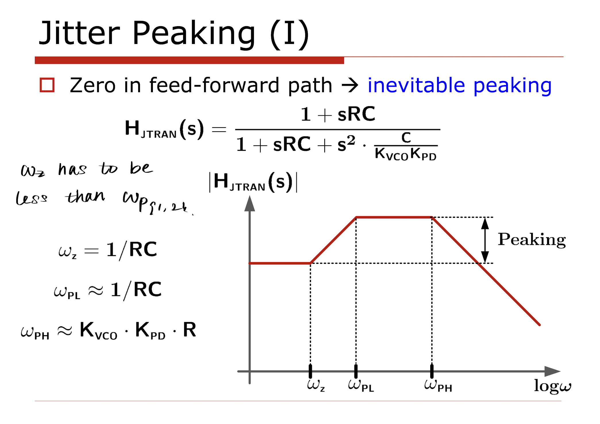
which is attributed to the inherent coupling between the two-integrator-induced stability and the feedforward zero. This doesn’t seem like a big problem if we were to use CDR to receive data, but it will become a bigger problem if CDR is used as active repeaters.
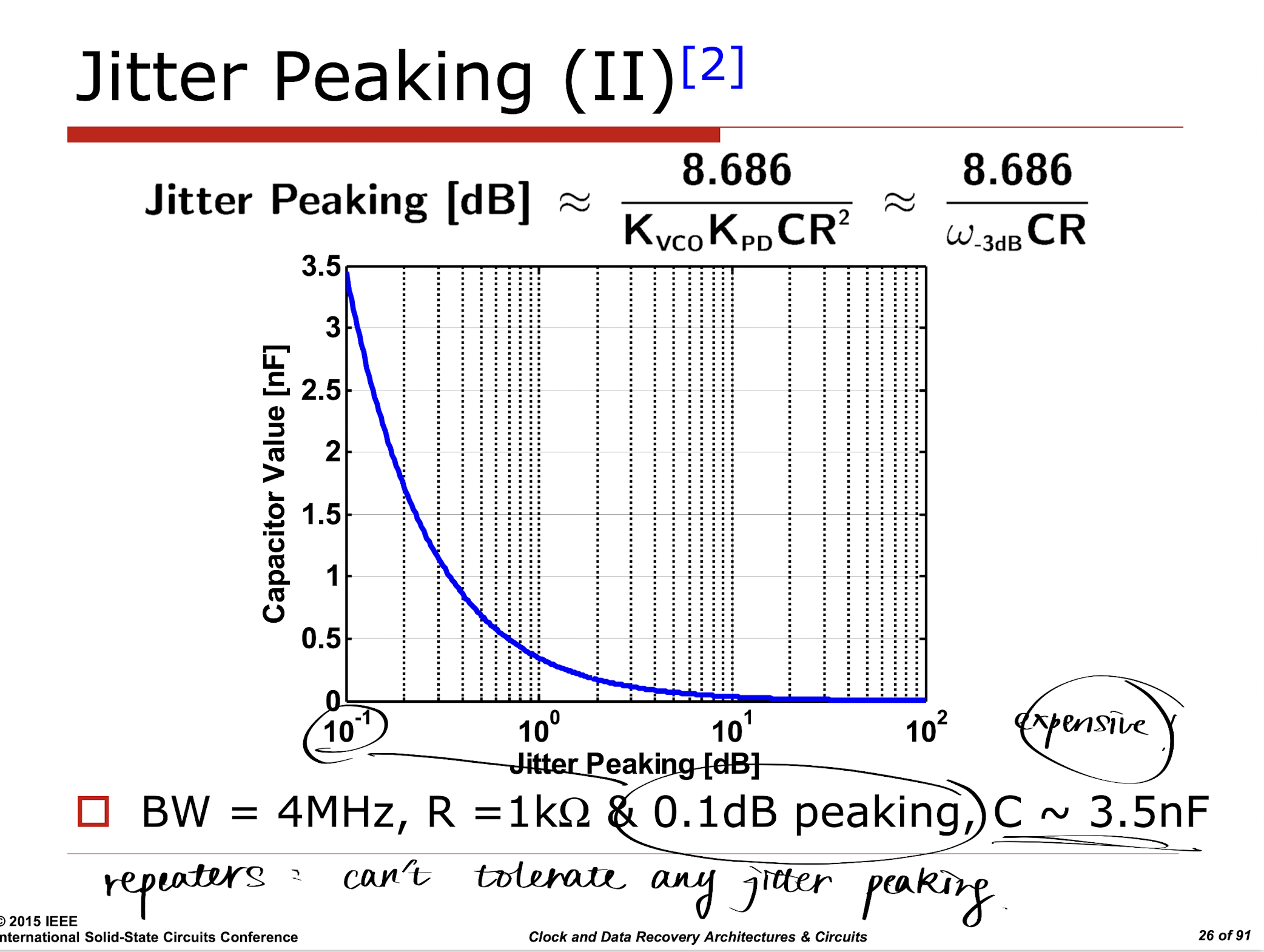
In order to reduce peaking, we would like to make the system much much more overdamped. This requires enlarging the damping factor $\zeta$, which can be achieved by increasing the damping capacitor $C$. This scaling quickly consumes all of our chip area:
JTOL and JTRAN Coupling
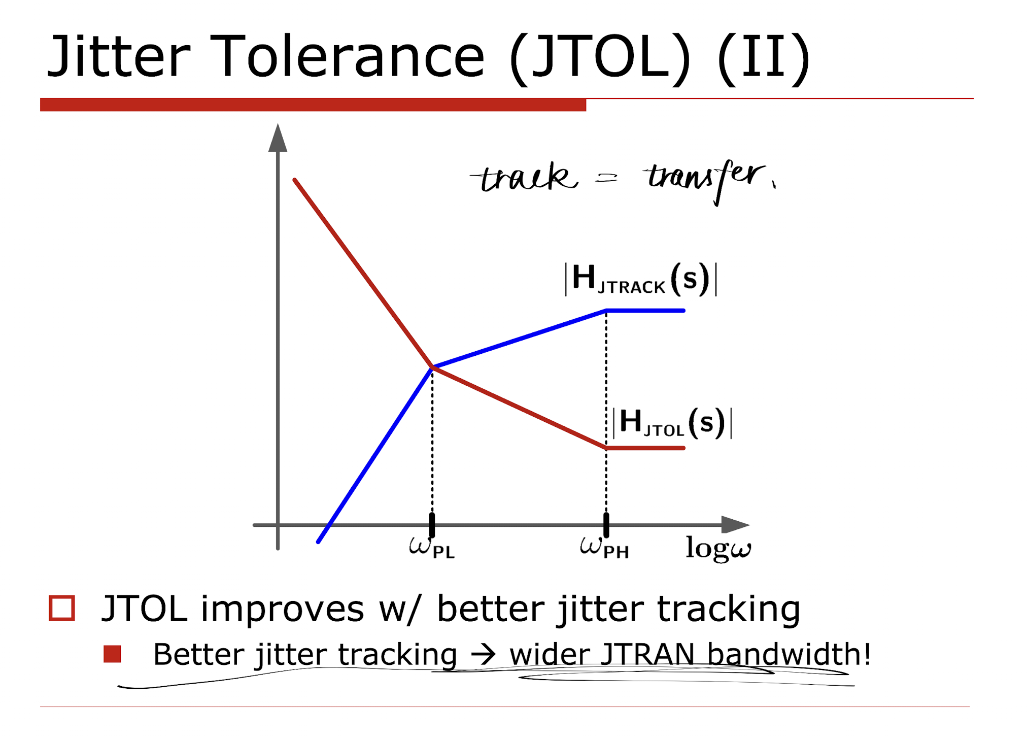
The second problem of the linear CDR is the coupling between JTOL and JTRAN.
In a word, the JTOL and JTRAN are coupled because they share the same loop. It can be derived that the jitter tracking bandwidth is:
$$ \omega_{JTRAN,-3dB} = K_{VCO}K_{PD}R $$Therefore, if we want to increase jitter tolerance, we will have to increase the jitter transfer bandwidth, which allows more jitter to pass through to the output.
Hogge PD non-idealities
There are also some non-idealities of the Hogge PD that we need to be aware of.
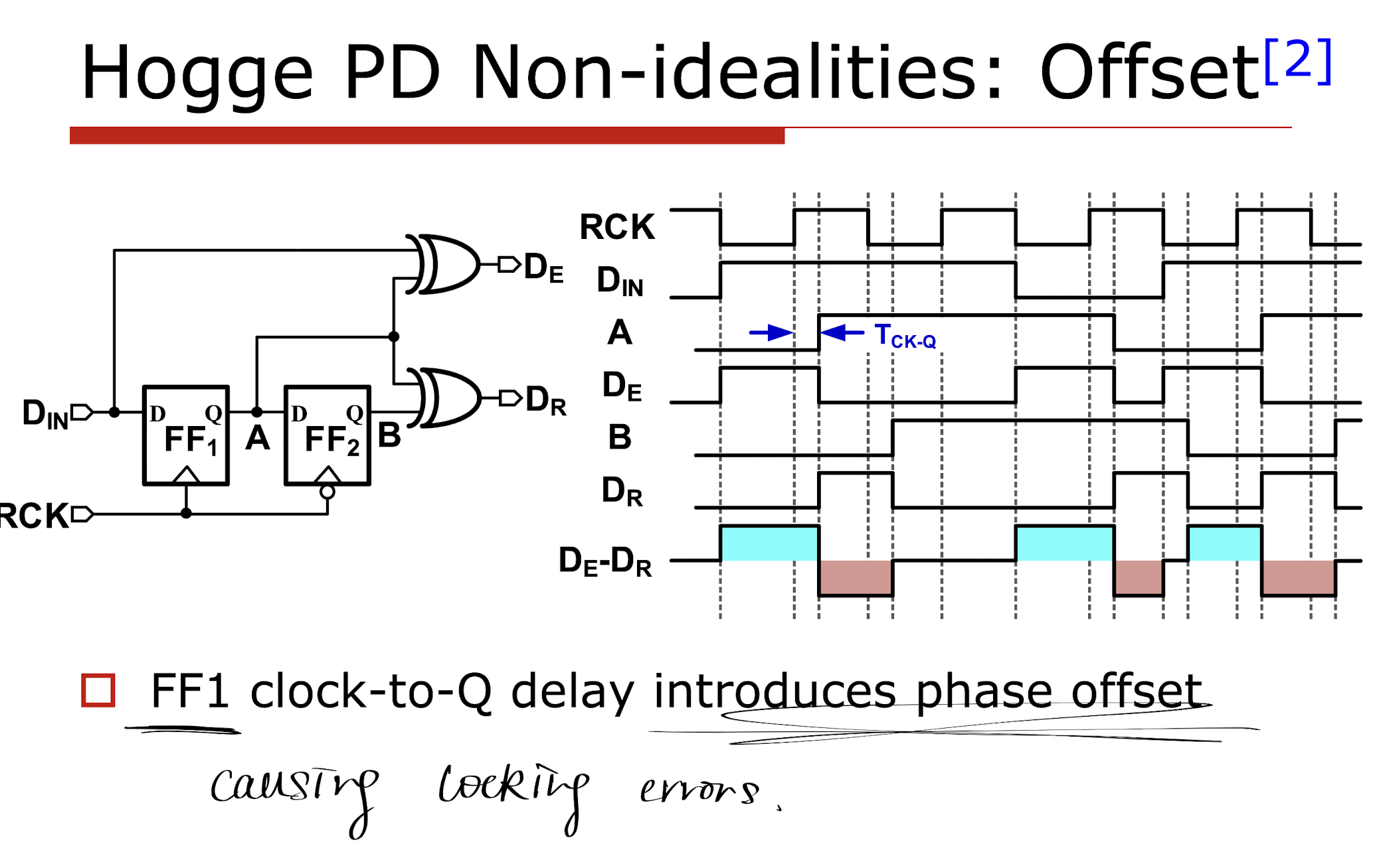
- Although $D_R$ always generates a half width pulse, $D_E$ does not always generate a pulse whose width is proportional to the phase difference, but will sometimes carry an offset given the CK-Q delay exists. One is able to insert a delay buffer in the $D_{IN}$ to the first XOR gate path, but such delay is hard to guarantee under PVT variations.
- Data-Dependent Jitter (DDJ) is another non-ideality. Unlike the PFD case in a type-2 PLL, $D_E$ and $D_R$ are not always in sync, and the control voltage at the VCO’s input will have a triangular spike when a data toggle happens.
Bang-Bang CDR
Therefore, we would now like to ask whether we can design a CDR that doesn’t have this offset problem? The answer is yes and the solution is known as the “Bang-Bang CDR”. Think about if we perform three consecutive samples of the data stream:
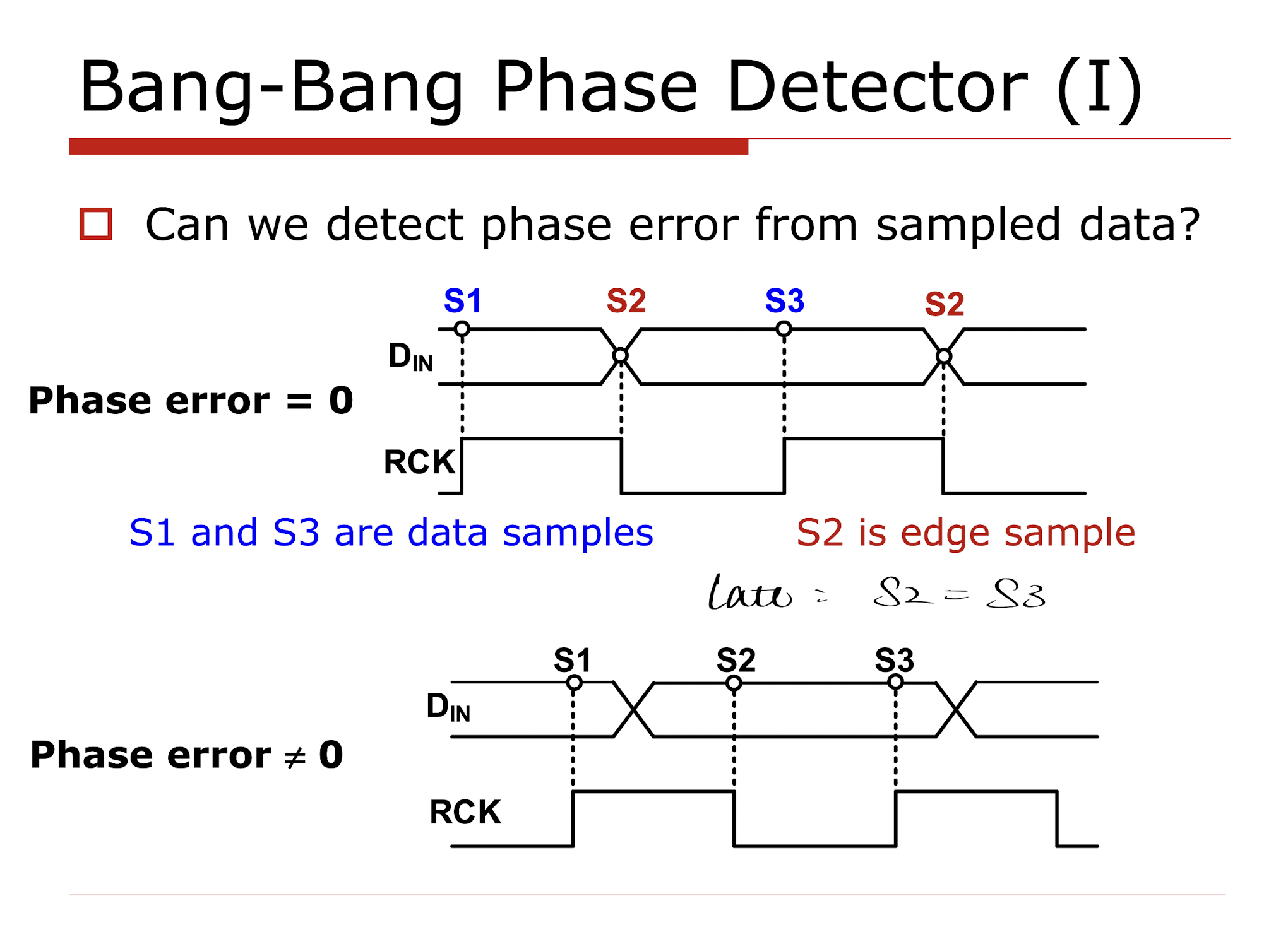
In this case S1 and S3 are the two consecutive data samples, and S2 is the edge sample in between. Think about the case if we have a data transition rendering S1 != S3, then we can use S2 to determine if the generated clock edge is more towards S1 or S3.
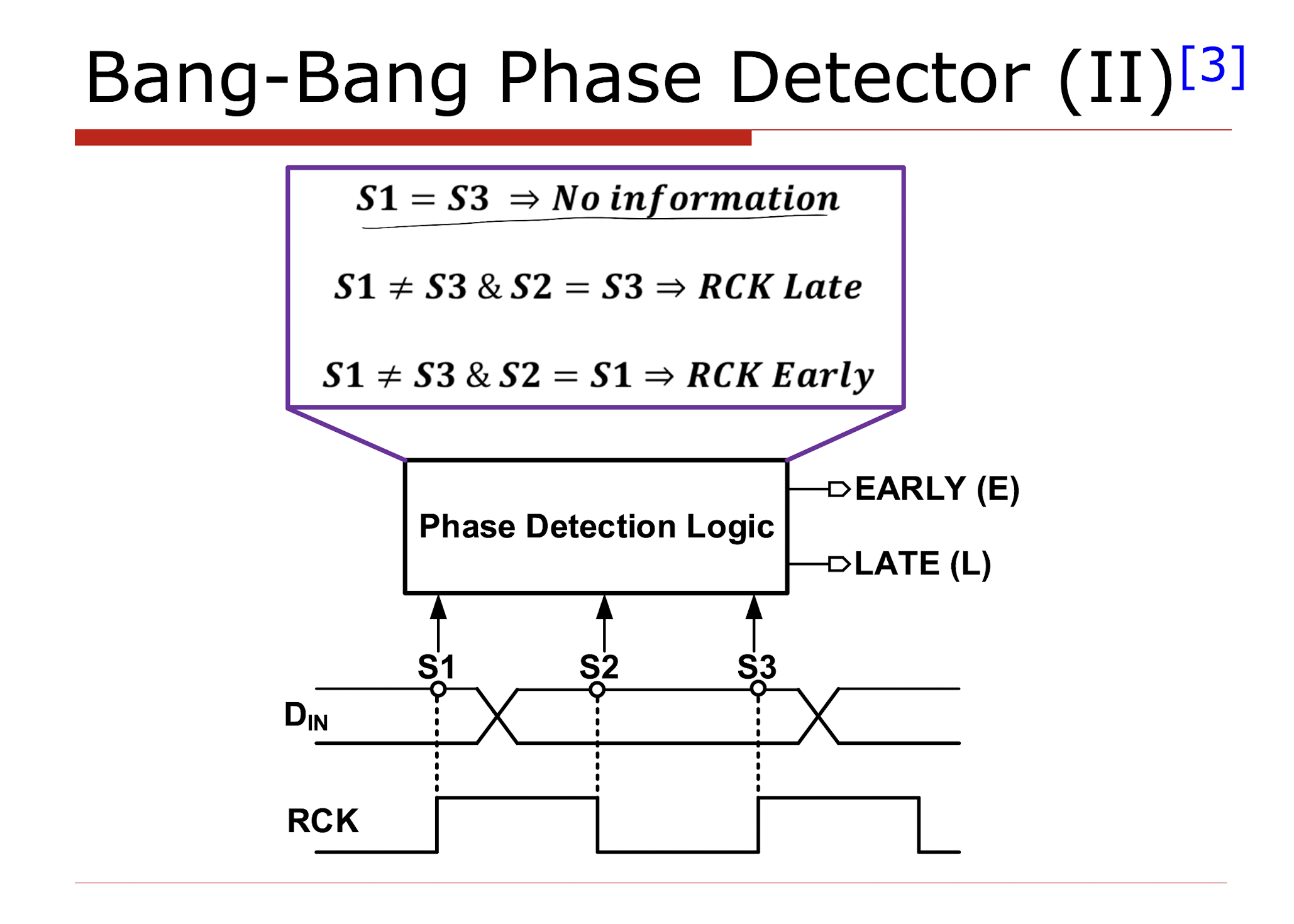
Like what is discussed in Nicola Da Dalt’s TCAS1 paper, the effective linearization can be achieved if the input is jittery.
Half Rate CDR
We discussed the concept of full-rate CDR so far where we use half of the transition to sample the edge crossing of the data stream, and the other half to sample the data. This is sometimes very expensive when we don’t have access to advanced PDKs and we’ll have to reduce the clock frequency to baud-rate instead. This is when the idea of half-rate CDR comes into play.
Instead of generating a clock that’s at the same frequency as the incoming data stream, we generate a clock that’s DDR at the same rate as the data. With the I (in-phase) and Q (quadrature) clock, we are able to sample the data stream at both edges of the clock, and therefore we can still recover the data stream.
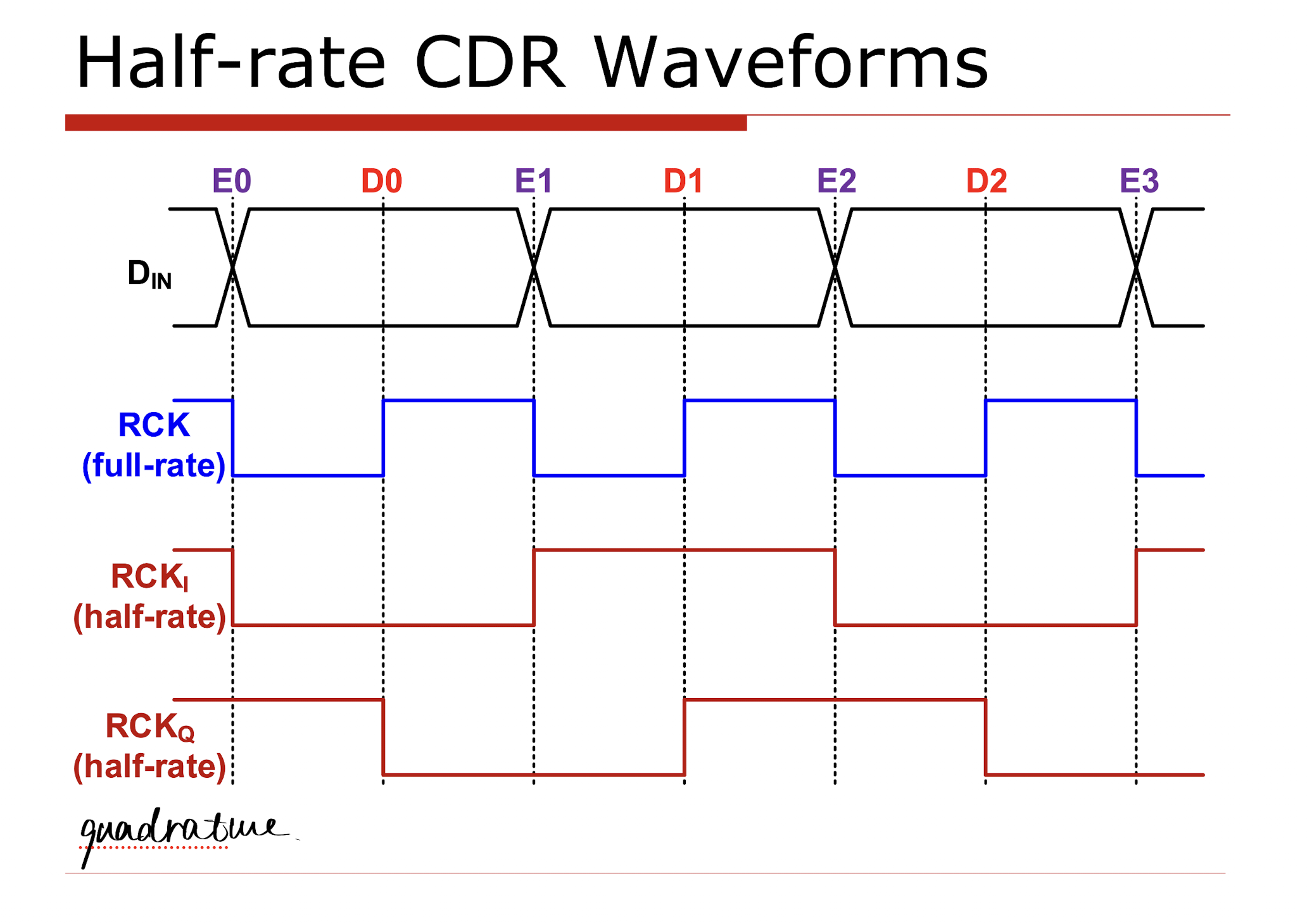
It’s easy to modify the full-rate CDR to a half-rate CDR using the following architecture:
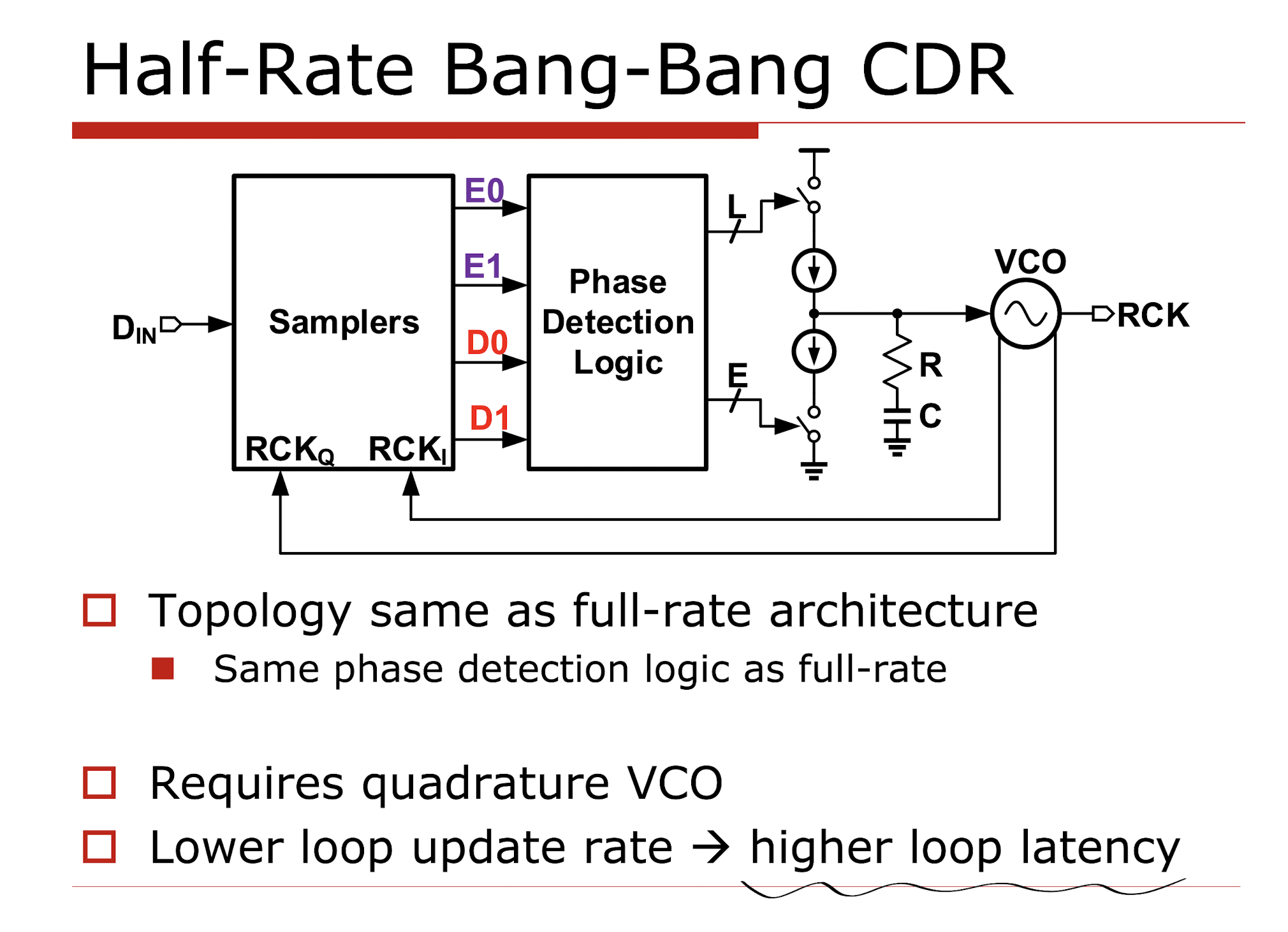
The thing to watch out for will be that 1. the oscillator has to generate both I and Q clocks, and 2. the loop latency is now higher and we’ll have to be careful about the loop stability.
Other problems associated with BBPD are:
- Limit cycles, if the input is pretty clean and most jitter is from the loop nonlinearity-induced limit cycling.
- Loop latency induced jitter peaking and JGEN.
Digital CDR and Hybrid CDR
Like that of a PLL, we are able to design CDR loops using a digital controller or in a hybrid manner. We’ll skip the details here.
If using a digital CDR, we’ll mainly have to match the digital gain factors to the analog gain factors. This saves capacitor area, but we’ll have to design a digitally-controlled oscillator (DCO), watch out for digital latency, and the loop quantization noise from the DCO.
Sometimes the proportional path latency and DCO quantization noise are not always desirable; this is when we would like to utilize a hybrid loop. Like other hybrid loops, we’ll have to carefully design the dual loop coupling in order to avoid offset-induced limit cycling and PVT variations from the analog path.
Prof. Pavan Hanumolu talks about more details about multi-path CDR and active repeaters; I omit the details here for simplicity and focus on CDR system only. If you are interested, please check out the slides I have at the top of this blog article.